可见光盲SiC紫外雪崩光电二极管  下载: 560次
High-sensitivity ultraviolet (UV) detectors are required in many critical applications such as corona discharge, missile plume detection, environmental monitoring, and non-line-of-sight communications. As an attractive candidate for weak UV signal detection, avalanche photodiodes (APDs) operating in Geiger mode exhibit promising performance, including small size, low dark current, and high multiplication gain. Wide-bandgap semiconductor materials, such as GaN and SiC, can effectively shield the influence of visible light and infrared light, showing obvious advantages in the field of UV detection. The defect density of GaN is relatively high, which leads to a generally high dark current in GaN APDs. In addition, the photoresponse behavior of GaN APDs under high pressure undergoes a significant red shift, and the cut-off wavelength is extended to 440 nm, indicating the loss of visible light blindness. In comparison, SiC can construct APDs with a much lower dark current than GaN owing to its excellent material epitaxial technology. However, there is still little research on the high-voltage photoresponse characteristics of SiC APDs, which are a key issue related to the background noise of the device. This work discusses the photoresponse behavior of SiC APD under high voltages. Moreover, owing to material defects, the size of the SiC APD is always below 300 μm, but a device with a large photosensitive area is needed to improve the detection sensitivity. Although some studies have reported SiC APDs with a diameter of 800 μm, the key parameter of the single-photon detection efficiency has not been successfully detected. In this study, low-dark-current SiC APDs with a diameter of 500 μm were successfully fabricated, and the devices exhibited single-photon detection performance. This is clearly a breakthrough in terms of the size of SiC APDs.
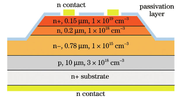
SiC APDs were fabricated on n-type 4H-SiC substrates (Fig. 1). The epi-structure from bottom to top consists of a 10 μm p+ layer (NA=3×1018 cm-3), a 0.78 μm n- multiplication layer (ND=1×1015 cm-3), a 0.2 μm n layer (ND=1×1018 cm-3), and a 0.15 μm n+ contact layer (ND=1×1019 cm-3). To suppress peak electrical field around device edge, the beveled mesa with a slope angle of 5° was obtained via photoresist reflow technique, and the mesa was etched down to the multiplication layer by inductively coupled plasma. The device surface was then passivated by thermal oxidation at 1050 ℃ in oxygen atmosphere followed by a 1 μm SiO2 layer deposited by plasma enhanced chemical vapor deposition at 350 ℃. The n and p type metal stacks, both based on Ni/Ti/Al/Au (35 nm/50 nm/100 nm/100 nm), were deposited by electron-beam evaporation. The devices were then annealed at 850 ℃ for 3 min in N2 ambient by rapid thermal annealing.
To analyze whether the SiC APDs still have visible light blindness in the Geiger mode, the photoresponse characteristics of the SiC APD are measured under high voltages. The results show that the response peak of SiC APD is always maintained at 280 nm when the voltage changes from 0% to 90% breakdown voltage (Fig. 3). It is proved that SiC APDs still exhibit visible-light blindness characteristics under high voltages. Owing to the properties of SiC, SiC APD enables the shielding effect of visible and infrared light, which greatly reduces the complexity, volume, and cost of the device. The activation energy of the 500 μm SiC APD is 0.131 eV (Fig. 5), which indicates that the tunneling effect is the main cause of the dark current. At present, the best SiC epitaxy technology can grow epitaxial wafers with a dislocation density of 1000-2000 cm-2. This implies that there are at least 2-4 dislocations in SiC APD with a diameter of 500 μm, which exacerbates defect-assisted tunneling and leads to a rapid increase in dark current. Therefore, the material defect density is a key problem that restricts the development of large-sized SiC APD. The dark current of the reported SiC APDs at 95% breakdown voltage has been calculated, and the comparison shows that the 500 μm SiC APDs fabricated in this work have a lower dark current (Fig. 7). Most importantly, the 500 μm SiC APDs in this work still have the single-photon detection capability. At a dark count rate of 1 Hz/μm2, the single photon detection efficiency of the device is 0.7%. The most recently reported largest diameter of SiC APD with single-photon detection capability was 300 μm. Although the single-photon detection efficiency of the 500 μm SiC APD reported in this work needs to be improved, a breakthrough in device size has been achieved.
In this work, by studying the photoresponse characteristics of SiC APDs under high voltages, it is proved that SiC APDs still exhibit visible light blindness in the avalanche breakdown state, which is more suitable for weak UV light detection than traditional Si or GaN. In addition, we successfully achieve a breakthrough in the photosensitive area of SiC APD and fabricate a large-sized SiC APD with single-photon detection performance. The dark current of the device is better than the existing level. However, to further improve the single-photon detection efficiency of large-sized SiC APDs, it is necessary to optimize the quality of SiC epitaxial wafers in future work.
1 引言
微弱紫外光探测在火灾预警、电晕检测、**预警和深空检测等领域中有着重要的应用前景[1-5]。雪崩光电二极管(APD)具有高量子效率、高增益和便于集成等优势,成为构建微弱紫外光探测器的首选器件。在材料方面,与Si相比,以GaN和SiC为代表的宽禁带半导体材料能够有效屏蔽可见光和红外光的影响,在紫外探测领域表现出明显优势。其中,GaN材料的缺陷密度比较大,这导致GaN APD的暗电流难以压制[6-7]。此外,GaN APD在高压下的光响应行为会发生明显红移,相关的研究表明:在0 V的工作电压下,GaN APD的峰值光响应位于364 nm处,截止波长为380 nm,而在90%击穿电压时,峰值光响应红移到370 nm处,截止波长也拓展到了440 nm[8]。因此,GaN APD在进行雪崩探测时将不再具有可见光盲特性。相比较而言,SiC凭借优异的材料外延技术,能够构建暗电流远低于GaN的APD器件,该器件是很有应用前景的一种微弱紫外光探测器件[9]。但目前关于SiC APD的高压光响应特性研究还鲜有报道,这是关系器件背景噪声的一个关键问题,因此本文将对器件高压下的光响应行为进行研究讨论。
另一方面,由于APD工作在雪崩击穿条件下,器件暗电流对材料的缺陷密度十分敏感,即便是低材料缺陷密度的SiC APD,器件直径也需要控制在300 μm以下[10-13]。但是,在进行微弱紫外光探测时,又需要器件具有大的感光面积以提高探测灵敏度。尽管有研究报道了直径为800 μm的SiC APD,但并未给出器件的单光子探测效率这一关键参数,这很可能与材料高缺陷密度引起的高的暗计数有关[14]。本文成功制备了直径为500 μm的低暗电流SiC APD,并且器件仍具有单光子探测性能。
2 器件制备
器件制备在n型4H-SiC衬底上,如
3 分析与讨论
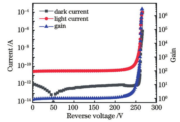
SiC APD在进行微弱紫外光探测时,需要工作在雪崩击穿状态下,为了分析器件工作时的可见光盲特性,我们表征了器件在高压下的光响应特性,
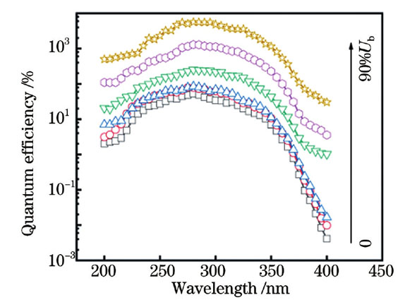
图 3. 不同电压下SiC APD的量子效率曲线
Fig. 3. Quantum efficiency curves of SiC APD under different voltages
为了提高器件的感光面积,我们同时制备了直径为300 μm和500 μm 的SiC APD。
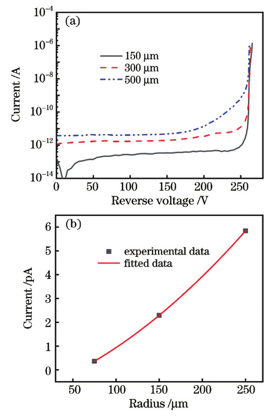
图 4. SiC APD的暗电流曲线。(a)不同直径SiC APD的暗电流曲线;(b)反向偏压为170 V时暗电流与半径的关系
Fig. 4. Dark current curves of SiC APD. (a) Dark current curves of SiC APDs with different diameters; (b) dark current as a function of radius at reverse voltage of 170 V
为了进一步分析器件体内漏电的原因,我们测试了500 μm SiC APD从室温到450 K的暗电流曲线,如
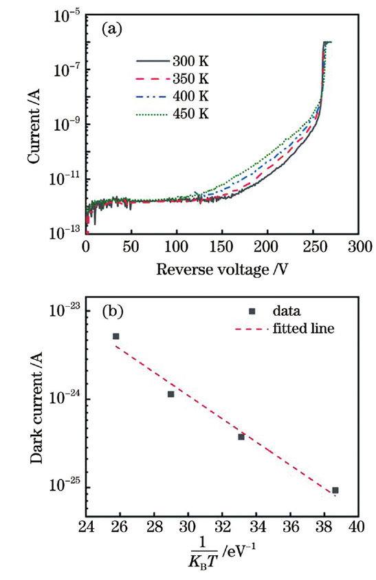
图 5. 500 μm SiC APD的暗电流曲线。(a)不同温度下的暗电流曲线;(b)反向偏压为200 V时的暗电流
Fig. 5. Dark current curves of 500 μm SiC APD. (a) Dark current curves at different temperatures; (b) dark current at reverse voltage of 200 V
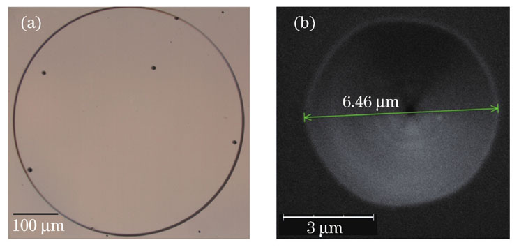
图 6. 缺陷图像。(a)光学显微镜图像;(b)扫描电子显微镜图像
Fig. 6. Images of defect. (a) Light microscope image; (b) scanning electron microscope image
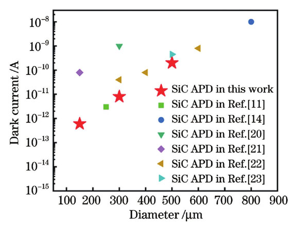
图 7. 不同SiC APD在95%击穿电压下的暗电流比较
Fig. 7. Comparison of dark currents of different SiC APDs at 95%Ub
为了表征器件的单光子探测能力,采用被动淬灭电路表征器件的暗计数和280 nm入射光下的光计数,并计算了单光子探测效率[20]。
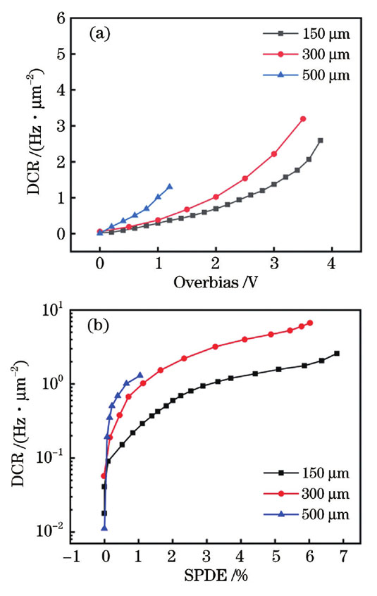
图 8. 不同尺寸SiC APD的暗计数和单光子探测效率。(a) 暗计数-过偏压曲线;(b)暗计数-单光子探测效率曲线
Fig. 8. Dark count rates and single photon detection efficiencies of SiC APDs with different sizes. (a) Dark count rate versus overbias; (b) dark count rate versus single photon detection efficiency
4 结论
通过研究SiC APD在高压下的光响应特性,证明了器件在雪崩击穿状态下仍具有可见光盲特性,比传统的Si材料或GaN材料更适于微弱紫外光探测。同时,还实现了SiC APD感光面积的突破,成功制备了具有单光子探测性能的大面积SiC APD,器件暗电流优于现有水平,但在今后的工作中仍需要继续优化SiC材料质量,以提高器件的单光子探测效率。
[1] Wang Y, Qian Y S, Kong X Y. Photon counting based on solar-blind ultraviolet intensified complementary metal-oxide-semiconductor (ICMOS) for corona detection[J]. IEEE Photonics Journal, 2018, 10(6): 1-19.
[2] 赵忆睿, 曹念文, 贾鹏程, 等. 紫外多波长激光雷达的臭氧和气溶胶同步观测研究[J]. 激光与光电子学进展, 2022, 59(16): 1601001.
[3] 袁兆林, 胡宇杰, 吕季辉, 等. ZnO纳米线阵列/PVK异质结紫外光探测器特性[J]. 光学学报, 2022, 42(22): 2204001.
[4] 孙立奇, 王登魁, 房丹, 等. CdSe量子点修饰ZnO微米线快速响应的紫外光电探测器[J]. 中国激光, 2022, 49(13): 1303001.
[5] 王江, 罗林保. 基于氧化镓日盲紫外光电探测器的研究进展[J]. 中国激光, 2021, 48(11): 1100001.
[6] Pau J L, McClintock R, Minder K, et al. Geiger-mode operation of back-illuminated GaN avalanche photodiodes[J]. Applied Physics Letters, 2007, 91(4): 041104.
[7] Cicek E, Vashaei Z, McClintock R, et al. Geiger-mode operation of ultraviolet avalanche photodiodes grown on sapphire and free-standing GaN substrates[J]. Applied Physics Letters, 2010, 96(26): 261107.
[8] Shen S C, Zhang Y, Yoo D W, et al. Performance of deep ultraviolet GaN avalanche photodiodes grown by MOCVD[J]. IEEE Photonics Technology Letters, 2007, 19(21): 1744-1746.
[9] Su L L, Zhou D, Lu H, et al. Recent progress of SiC UV single photon counting avalanche photodiodes[J]. Journal of Semiconductors, 2019, 40(12): 65-75.
[10] Vert A, Soloviev S, Sandvik P. SiC avalanche photodiodes and photomultipliers for ultraviolet and solar-blind light detection[J]. Physica Status Solidi (a), 2009, 206(10): 2468-2477.
[11] Bai X G, Liu H D, McIntosh D C, et al. High-detectivity and high-single-photon-detection-efficiency 4H-SiC avalanche photodiodes[J]. IEEE Journal of Quantum Electronics, 2009, 45(3): 300-303.
[12] Zhou D, Liu F, Lu H, et al. High-temperature single photon detection performance of 4H-SiC avalanche photodiodes[J]. IEEE Photonics Technology Letters, 2014, 26(11): 1136-1138.
[13] Li L H, Zhou D, Lu H, et al. 4H-SiC avalanche photodiode linear array operating in Geiger mode[J]. IEEE Photonics Journal, 2017, 9(5): 6804207.
[15] Guo X Y, Beck A L, Li X W, et al. Study of reverse dark current in 4H-SiC avalanche photodiodes[J]. IEEE Journal of Quantum Electronics, 2005, 41(4): 562-567.
[16] Maimon S, Wicks G W. nBn detector, an infrared detector with reduced dark current and higher operating temperature[J]. Applied Physics Letters, 2006, 89(15): 151109.
[17] Ji X L, Liu B Q, Xu Y, et al. Deep-level traps induced dark currents in extended wavelength InxGa1-xAs/InP photodetector[J]. Journal of Applied Physics, 2013, 114(22): 224502.
[18] Yang S, Zhou D, Cai X L, et al. Analysis of dark count mechanisms of 4H-SiC ultraviolet avalanche photodiodes working in Geiger mode[J]. IEEE Transactions on Electron Devices, 2017, 64(11): 4532-4539.
[19] Su L L, Zhou D, Liu Q, et al. Effect of a single threading dislocation on electrical and single photon detection characteristics of 4H-SiC ultraviolet avalanche photodiodes[J]. Chinese Physics Letters, 2020, 37(6): 068502.
[20] Zhou X Y, Tan X, Lü Y J, et al. Single-photon-counting performance of 4H-SiC avalanche photodiodes with a wide-range incident flux[J]. IEEE Photonics Technology Letters, 2020, 32(14): 847-850.
[21] Zhou X Y, Tan X, Lü Y J, et al. 128-pixel arrays of 4H-SiC UV APD with dual-frequency PECVD SiNx passivation[J]. Optics Express, 2020, 28(20): 29245-29252.
[23] Cha H Y, Soloviev S, Zelakiewicz S, et al. Temperature dependent characteristics of nonreach-through 4H-SiC separate absorption and multiplication APDs for UV detection[J]. IEEE Sensors Journal, 2008, 8(3): 233-237.
杨成东, 苏琳琳, 夏开鹏, 马文烨. 可见光盲SiC紫外雪崩光电二极管[J]. 中国激光, 2022, 49(24): 2401003. Chengdong Yang, Linlin Su, Kaipeng Xia, Wenye Ma. SiC Visible Light Blindness UV Avalanche Photodiodes[J]. Chinese Journal of Lasers, 2022, 49(24): 2401003.
