Chinese Optics Letters, 2020, 18 (4): 042401, Published Online: Mar. 18, 2020  

Metalens for coaxial double wavelength focusing Download: 730次

Author Affiliations
School of Physics and Opto-Electronics Engineering, Ludong University, Yantai 264025, China
Abstract
We propose a metalens for coaxial double wavelength focusing. One focusing spot is a circular solid spot, and the other focusing spot is a doughnut-shaped spot that is circling the solid spot. The designed metalens was composed of a meta-molecular nanostructured cell array. Each meta-molecular nanostructured cell was divided into four squares. Two slots with exactly the same shape, but usually with the rotation angle measured clockwise from the positive x axis, are etched into the gold film in two diagonally connected squares. Another two slots with the same shape but with the rotation angle measured counter-clockwise from the positive x axis are etched into another two diagonally connected squares in the same cell. The lasers with two different wavelengths are transformed into right-handed and left-handed circularly polarized beams, respectively. The two sets of slots with different azimuthal rotations modulated the phases of incident right-handed and left-handed circularly polarized beams independently. The numerical simulation with finite-difference time-domain (FDTD) software was carried out, and the experimental verification was also implemented. Both the experimental result and the numerical simulation agree well with the theoretical design.

Tightly focused far-field spots have many applications in various fields such as laser precision processing, fluorescent microscopic imaging, lithography, optical data storage, and micro-particle manipulation. The spot size is usually measured with its full width at half-maximum (FWHM). However, the Abbe’s diffraction limit strongly restricts their minimum spot size. Fighting against the diffraction limit has always been the topic optical scientists make the effort to tackle. Mainly, there are two approaches to break through the diffraction limit. Conventionally, we usually obtain the far-field spot size below the diffraction limit by comprehensively modulating the amplitude, phase, and polarization distribution of the laser beam at the entrance pupil of the objective with a high numerical aperture. Because of its axial symmetry of polarization, the radially polarized beam is preferred to obtain a spot size smaller than the diffraction limit[1]. In 2003, Quabis’s group from Germany used the annular aperture to block the central part of the light beam in the focusing of radially polarized beams[2]. The central blocking of incoming light increased the ratio of the longitudinally polarized component to the transversely polarized component in the focal volume and made the size of the focusing spot smaller. In their work, the annular aperture acts as an amplitude filter. In 2008, Wang from the Singapore Data Storage Institute designed a multiple binary annular phase mask to modulate the incident radially polarized beam[3]. The FWHM of the focusing spot size is around 0.42λ. It is a light needle with the focal depth of more than 4λ. The long needle-shaped spot also makes the off-focus insensitive in applications.

Another approach to break through Abbe’s diffraction limit is the so-called super-oscillatory lens. The super-oscillatory lens is first proposed theoretically, to the best of our knowledge, by Berry from the University of Bristol in 2006[4,5]. In 2012, Zheludev’s group from the University of Southampton designed and fabricated a super-oscillatory lens composed of a series of concentric binary amplitude rings[6,7]. They obtained a spot size of 185 nm (0.29λ) in the oil-immersion medium. However, limited by its intrinsic physical nature of the super-oscillatory lens, it will inevitably cause strong side-lobes besides the main peak. To inhibit the strong side-lobes, the research group from Singapore National University designed and fabricated a binary amplitude-type planar super-critical lens[8]. When it was illuminated by an azimuthally polarized vortex beam with a wavelength of 633 nm, they obtained the focusing spot with the transverse size of 265 nm (0.42λ). Compared with the super-oscillatory lens, the intensity of the side-lobes is greatly reduced. The super-critical lens has now been used in a label-free confocal scanning microscope to enhance the imaging resolution[7].

In the field of scanning fluorescent microscopic imaging, the resolution is directly determined by the obtainable minimum focusing spot size. To circumvent this limit, Hell invented stimulated emission depletion microscopy (STED)[9,10]. He introduced a second laser beam with a different wavelength. It is imposed on a vortex phase modulation and is focused into a doughnut-shaped spot that acts as depleting stimulated fluorescent molecules. It in turn greatly reduces the size of the single pixel emitting fluorescent light. The STED system usually requires careful coaxial tuning of two laser beams along with a separate vortex phase plate and a high numerical objective. The misalignment of the optical elements will deform and damage the circular symmetry of the doughnut-shaped spot. It seriously compromises the resolution of the STED system.

In recent years, metasurfaces have attracted great attention attributed to their distinguished features, versatile functionality, easy integration, and relatively simple fabrication. Metasurfaces are usually composed of an ultrathin, space-variant, and nanostructured subwavelength cell array acting as local polarization, amplitude, or phase modulation pixels[1117" target="_self" style="display: inline;">17]. By carefully designing the nanostructure with deep subwavelength resolution, lots of metasurface devices such as quarter wave plates[18], optical vortex plates[1921" target="_self" style="display: inline;">–21], and metasurface holograms[2226" target="_self" style="display: inline;">26] have been reported.

In this study, we propose and demonstrate a metalens for coaxial double wavelength focusing, which can be used in the STED scheme. Due to the nature of the method, it guarantees the coaxial feature, the optical stability, and the circular symmetry of the doughnut-shaped spot.

We assume that the first laser with wavelength λ1 is supposed to be focused into a circular solid spot, and a second laser with wavelength λ2 is supposed to be focused coaxially into a doughnut-shaped spot. The phase of the first laser has to be modulated following Eq. (1), and the phase of the second laser has to be modulated following Eq. (2): ψ1(x,y)=2πλ1(x2+y2+f2f),ψ2(x,y)=2πλ2(x2+y2+f2f)+ϕ(x,y),where f is the common focal length of the metalens for two lasers. Figure 1(a) is a graphic illustration for phase modulation described by Eq. (1). ϕ(x,y) is an azimuthal angle, which is equal to the vortex phase with a topological charge of one. Figure 1(b) is a vortex phase for ϕ(x,y). Figure 1(c) is a graphic illustration for phase modulation described by Eq. (2).
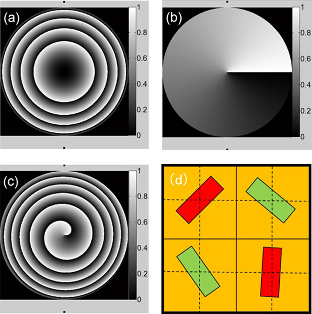
Fig. 1. Design scheme of the metalens for coaxial double wavelength focusing. (a) The phase modulation for the laser with a wavelength of λ1; (b) the phase modulation of a vortex with a topological charge of one; (c) the phase modulation combining (a) and (b) for the laser with a wavelength of λ2; (d) the meta-molecular structure unit.

下载图片 查看所有图片

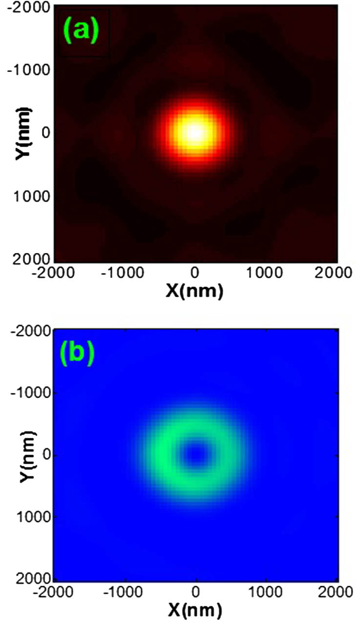
The metalens is composed of a square cell array. Each square cell is further divided into four small squares, as shown in Fig. 1(d). Four slots with the same width and length are etched into the gold film deposited on a SiO2 substrate. However, the red slots in the whole metalens designed for the first laser are rotated according to θ1(x,y)=ψ1(x,y)/2, while the green slots designed for the second laser are rotated according to θ2(x,y)=ψ2(x,y)/2. If the rotational direction of the red slots is clockwise, then the rotation direction of the green slots is designed to be counter-clockwise. Meanwhile, the rotation direction of the polarization of the circularly polarized beam with wavelength λ1 has to be the same as the red slots in order to achieve the Pancharatnam–Berry phase modulation. Similarly, the rotation direction of the polarization of the circularly polarized beam with wavelength λ2 has to be the same as the green slots. If the rotation directions of the red slots and green slots are exchanged, accordingly, the rotation directions of polarizations of circularly polarized beams with wavelengths λ1 and λ2 should also be exchanged. So, there are two schemes for the slot rotation directions and polarization rotation directions of circularly polarized beams. Figure 2 shows the designed two-dimensional nanostructure for a relatively small metalens 24.6μm×24.6μm. The other parameters are as follows: λ1=633nm, λ2=532nm, and f=25μm. It is imported into the three-dimensional model of finite-difference time-domain (FDTD) solutions. The thickness of the gold film is 150 nm. A right-handed circularly polarized beam and a left-handed circularly polarized beam are incident on the metalens from the substrate side. We first obtained electric field distribution on the monitor located 10 nm away from the front surface of the metalens. Then, we calculate the far-field intensity distribution at the focal plane using script command “farfieldexact3D”. Figure 3(a) is the circular solid spot generated by the first laser with wavelength λ1. The color is similar to the true color of the laser. The FWHM of the spot is around 320 nm. Figure 3(b) is the doughnut-shaped focusing spot with a diameter of 1050 nm. Actually, when two laser beams are incident on the whole metalens, the laser with wavelength λ1 will inevitably pass through the green-filled slots, and the laser with wavelength λ2 will pass through the red-filled slots. However, both of them will diverge almost randomly to all directions and will not collectively focus to the effective spots. It assumingly causes weak background and also greatly decreases the light efficiency. The diffraction efficiency is around 13.5% for the circular solid spot with wavelength λ1=633nm and 14.2% for the doughnut-shaped spot with wavelength λ2=532nm. The difference between the two spots arises from the different wavelengths, while the green slots and red slots have exactly the same width and length.
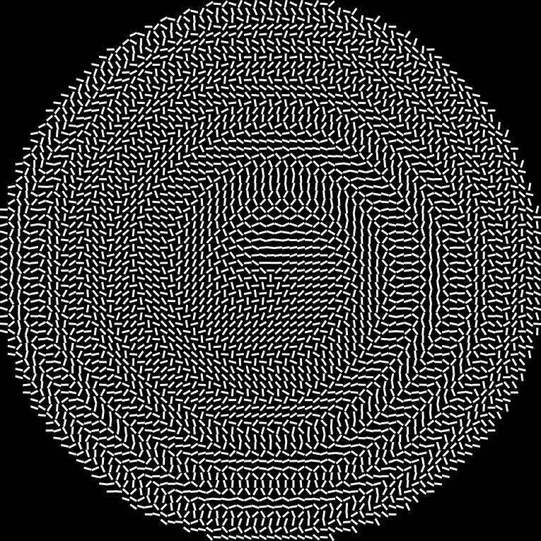
Fig. 2. Schematic diagram of the designed metalens for coaxial double wavelength focusing.
下载图片 查看所有图片

Fig. 3. FDTD-simulated focusing spot for designed metalens. (a) The circular solid spot for the first laser with λ1; (b) the doughnut-shaped focusing spot for second laser with λ2.

下载图片 查看所有图片

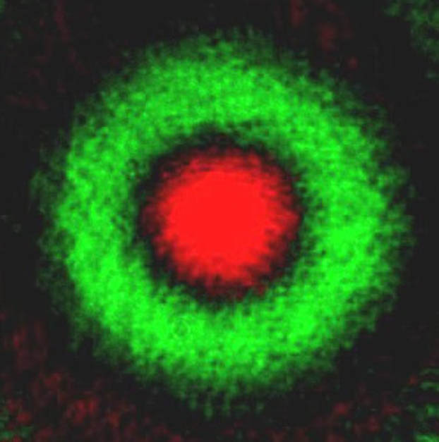
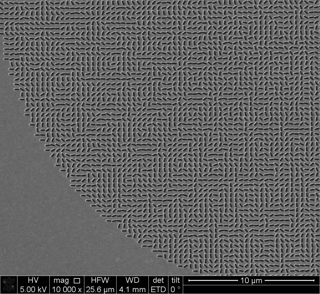
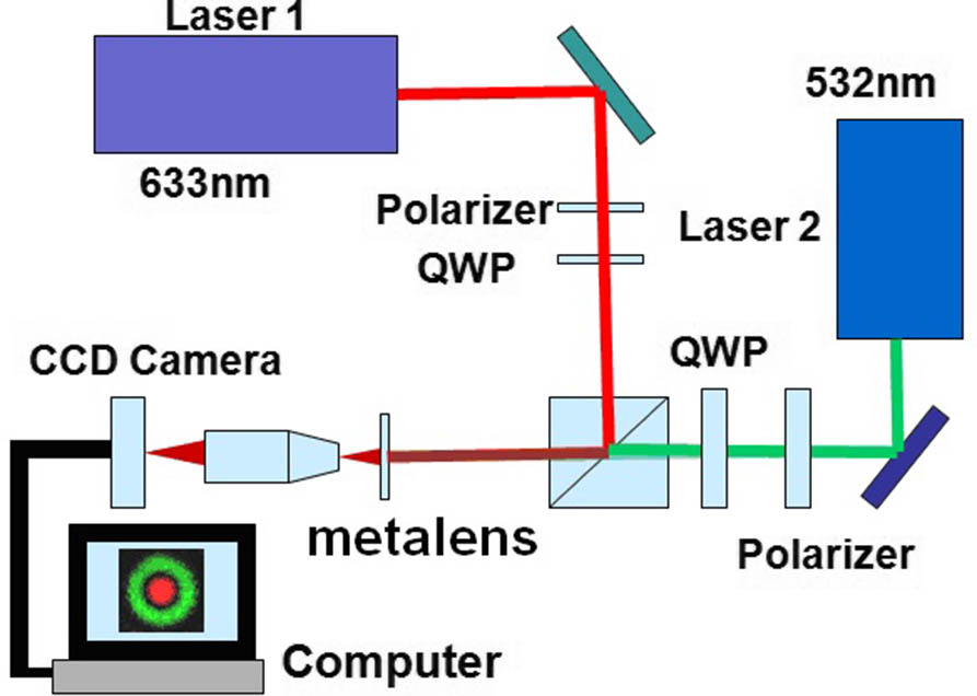
To verify the design effectiveness of the metalens, we prepared a gold film on the substrate with the electron beam evaporation technique, and the thickness of the film is 150 nm. Then, the sample metalens is fabricated by a focused ion beam (FIB, EFI Nanolab600, Helios). The size of the experimental sample (100μm×100μm) is much larger than that of the simulation sample. The focal length is 120μm. Figure 4 is the local magnified scanning electron microscope (SEM) image of the fabricated metalens. The scale bar at the right-bottom corner of the image is 10μm. Figure 5 illustrates the schematic diagram of the experimental setup. The two laser beams (633 nm and 532 nm) are transformed into left-handed circularly polarized light and a right-handed circularly polarized beam as demanded in the design. The metalens is mounted on a three-dimensional scanning stage. The objective for observing the focal spot is from Olympus (×100,NA=0.9). The camera is from Edmund (EO-5012). Figure 6 shows the result. We see that the red solid circular spot is strictly coaxial with the green doughnut-shaped spot. Actually, it is insured by both the design method and FIB super-resolution fabrication process. This metalens will also guarantee the generation of a circularly symmetrical doughnut-shaped spot. The result agrees well with the expectation.

Fig. 4. Local magnified SEM image of the fabricated metalens.

下载图片 查看所有图片

Fig. 5. Experimental setup for verifying the functionality of the designed metalens.

下载图片 查看所有图片

Fig. 6. Experimental result that is captured by a CCD camera.

下载图片 查看所有图片

We have demonstrated the design scheme of a metalens for coaxial double wavelength focusing. Both the numerical simulation of the FDTD solution and experimental verification show that the design scheme is reasonable. The advantage of the metalens lies in that the vortex phase plate and conventional objective are combined into one integrated metalens. This insures the coaxial demand of two spots and the stability of the STED system. Another advantage of the metalens compared with the conventional objective made of glass and metal is that it has a very small size and weight. The small size may help to realize the portability and instrument minimization. The small weight is beneficial to the easy and precise scanning of the relevant STED system.

References

[1] YoungworthK. S.BrownT. G., Opt. Express7, 77 (2000).OPEXFF1094-4087

[2] DornR.QuabisS.LeuchsG., Phys. Rev. Lett.91, 233901 (2003).PRLTAO0031-9007

[3] WangH.ShiL.LukyanChukB.SheppardC.ChongC. T., Nat. Photon.2, 501 (2008).NPAHBY1749-4885

[4] BerryM. V., J. Phys. A: Math. Theor.46, 205203 (2013).JPAMB51751-8113

[5] BerryM. V.PopescuS., J. Phys. A: Math. Theor.39, 6965 (2006).JPAMB51751-8113

[6] RogersE. T. F.ZheludevN. I., J. Opt.15, 094008 (2013).

[7] RogersE. T. F.LindbergJ.RoyT.SavoS.CardJ. E.DennisM. R.ZheludevN. I., Nat. Mater.11, 432 (2012).NMAACR1476-1122

[8] QinF.HuangK.WuJ.JiaoJ.LuoX.QiuC.HongM., Sci. Rep.5, 9977 (2015).SRCEC32045-2322

[9] HellS. W., Nat. Biotechnol.21, 1347 (2003).NABIF91087-0156

[10] HellS. W.WichmannJ., Opt. Lett.19, 780 (1994).OPLEDP0146-9592

[11] KhorasaninejadM.ShiZ.ZhuA. Y.ChenW. T.SanjeevV.ZaidiA.CapassoF., Nano. Lett.17, 1819 (2017).

[12] ChoiC.KimS.-J.YunJ.-G.SungJ.LeeS.-Y.LeeB., Chin. Opt. Lett.16, 050009 (2018).CJOEE31671-7694

[13] YanJ.GuoY.PuM.LiX.MaX.LuoX., Chin. Opt. Lett.16, 050003 (2018).CJOEE31671-7694

[14] HuangL.ChenX.MühlenberndH.ZhangH.ChenS.BaiB.TanQ.JinG.CheahK.-W.QiuC.-W.LiJ.ZentgrafT.ZhangS., Nat. Commun.4, 2808 (2013).NCAOBW2041-1723

[15] CuiY.ZhengG.ChenM.ZhangY.YangY.TaoJ.LiZ., Chin. Opt. Lett.17, 111603 (2019).CJOEE31671-7694

[16] GroeverB.ChenW. T.CapassoF., Nano. Lett.17, 4902 (2017).

[17] KhorasaninejadM.ChenW. T.DevlinR. C.OhJ.ZhuA. Y.CapassoF., Science352, 1190 (2016).SCIEAS0036-8075

[18] YuN.AietaF.GenevetP.KatsM. A.GaburroZ.CapassoF., Nano Lett.12, 6328 (2012).

[19] GenevetP.YuN.AietaF.LinJ.KatsM. A.BlanchardR.ScullyM. O.GaburroZ.CapassoF., Appl. Phys. Lett.100, 013101 (2012).APPLAB0003-6951

[20] HeJ.WangX.HuD.YeJ.FengS.KanQ.ZhangY., Opt. Express21, 20230 (2013).OPEXFF1094-4087

[21] YuN.GenevetP.KatsM. A.AietaF.TetienneJ.-P.CapassoF.GaburroZ., Science334, 333 (2011).SCIEAS0036-8075

[22] ZhaoW.LiuB.JiangH.SongJ.PeiY.JiangY., Opt. Lett.41, 147 (2016).OPLEDP0146-9592

[23] WanW.GaoJ.YangX., ACS Nano10, 10671 (2016).ANCAC31936-0851

[24] WangB.DongF.LiQ.-T.YangD.SunC.ChenJ.SongZ.XuL.ChuW.XiaoY.-F.GongQ.LiY., Nano. Lett.16, 5235 (2016).

[25] WangQ.XuQ.ZhangX.TianC.XuY.GuJ.TianZ.OuyangC.ZhangX.HanJ.ZhangW., ACS Photon.5, 599 (2018).

[26] HuangY.-W.ChenW. T.TsaiW.-Y.WuP. C.WangC.-M.SunG.TsaiD. P., Nano. Lett.15, 3122 (2015).

Jiannong Chen, Baodong Wang, Linwei Zhu, Jing Han, Qinfeng Xu. Metalens for coaxial double wavelength focusing[J]. Chinese Optics Letters, 2020, 18(4): 042401.
引用该论文: TXT   |   EndNote

相关论文

加载中...

关于本站 Cookie 的使用提示

中国光学期刊网使用基于 cookie 的技术来更好地为您提供各项服务,点击此处了解我们的隐私策略。 如您需继续使用本网站,请您授权我们使用本地 cookie 来保存部分信息。
全站搜索
您最值得信赖的光电行业旗舰网络服务平台!