Author Affiliations
Abstract
1 State Key Laboratory of Integrated Optoelectronics, Institute of Semiconductors, Chinese Academy of Sciences, Beijing 100083, China
2 Center of Materials Science and Optoelectronics Engineering, University of Chinese Academy of Sciences, Beijing 100049, China
3 School of Electronic, Electrical and Communication Engineering, University of Chinese Academy of Sciences, Beijing 100049, China
4 College of Materials Science and Optoelectronic Technology, University of Chinese Academy of Sciences, Beijing 100049, China
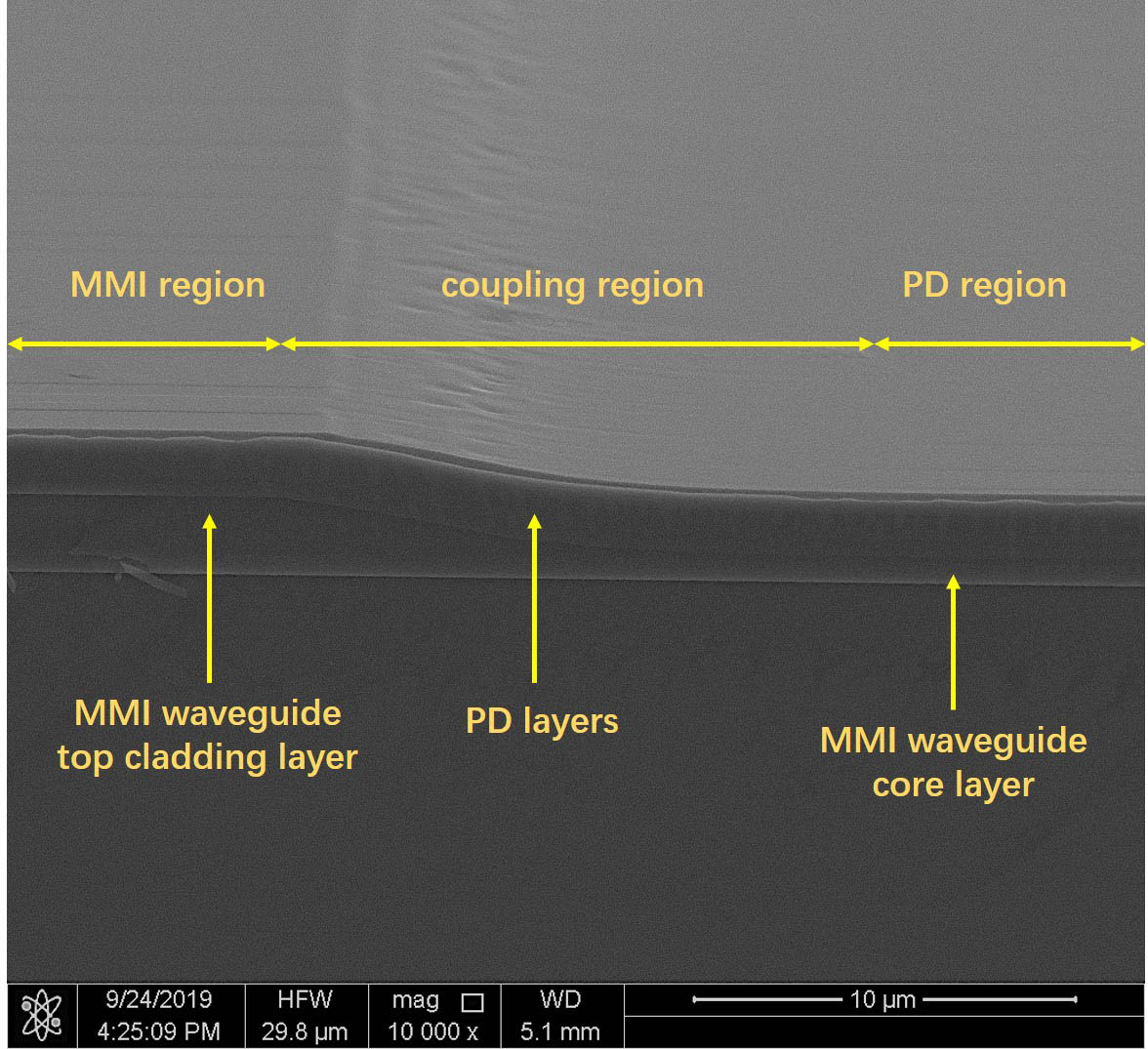
A quadrature phase-shift keying (QPSK) coherent photodetector chip consisting of a multimode interference 90° optical hybrid and a four-channel evanescent photodetector array is designed and fabricated with its photo-response in the L-band characterized. The metal organic chemical vapor deposition regrowth method is adopted to realize active–passive monolithic integration. The chip exhibits a low dark current below 100 nA for each photodetector in the array, a low excess loss of 0.85 dB, a common mode ratio rejection better than 13.6 dB, and a phase deviation within over the 40 nm wavelength span.
hybrid photodetectors monolithic integration photo-response Chinese Optics Letters
2023, 21(1): 011301
1 中国科学院半导体研究所 集成光电子学国家重点实验室,北京 100083
2 中国科学院大学 材料科学与光电技术学院,北京 100049
3 中国科学院大学 电子电器与通信工程学院,北京 100049
在越来越多的光子计数应用中,用于近红外光波长领域的单光子探测器受到广泛关注。例如在量子信息处理、量子通信、3D激光测距(LiDAR)、时间分辨光谱等光子计数应用领域。文中设计并展示了用于探测1 550 nm波长光子的InGaAs/InP单光子雪崩二极管(SPAD)。这种SPAD 采用分离吸收、过渡、电荷和倍增区域结构 (SAGCM),在盖革模下工作时具有单光子灵敏度。SPAD的特性包括随温度范围223~293 K变化的击穿电压、暗计数率、单光子检测效率和后脉冲概率。25 μm 直径的 SPAD 显示出一定的温度相关性,击穿电压随温度的变化率约为100 mV/K。当SPAD在盖革模式下温度为223 K工作时,在暗计数率为4.1 kHz,后脉冲概率为3.29%的基础上,对1 550 nm光子实现了21%的单光子探测效率。文中还分析和讨论了SPAD温度相关性的单光子探测效率、暗计数率和后脉冲概率的来源和物理机制。这些机制分析、讨论和计算可以为SPAD的设计和制备提供更多的理论支持和依据。
单光子探测器 温度相关性 光子探测效率 暗计数率 后脉冲概率 single-photon detector temperature dependency photon detection efficiency dark count rate after pulse probability 红外与激光工程
2021, 50(11): 20210453
1 中国科学院半导体研究所 集成光电子学国家重点实验室, 北京 100083
2 中国科学院大学 电子电气与通信工程学院, 北京 100049
3 中国电子科技集团公司第四十四研究所 化合物半导体光电子事业部, 重庆 400060
通过测量平面型InGaAs/InP雪崩光电二极管闭管扩散器件帽层InP中Zn杂质的分布, 拟合出掺杂浓度随扩散深度的变化函数, 并且利用离化积分研究不同倍增层厚度下的最佳刻蚀坑深度和最佳刻蚀方法.结果表明在帽层深度不变的情况下, 最佳刻蚀坑深度会随着倍增层厚度而变化, 当倍增层厚度为1 μm左右时刻蚀坑深度在0.1~0.3 μm之间.采取反应离子刻蚀可以获得良好的刻蚀坑形貌, 有利于边缘击穿的抑制.
雪崩光电二极管 光探测器 离化积分 电场击穿 刻蚀 反应离子刻蚀 盖革计数 Avalanche photodiodes Photodetectors Ionization integral Electric breakdown Etching Reactive ion etching Geiger counters
1 中国科学院半导体研究所 集成光电子学国家重点实验室, 北京 100083
2 中国科学院大学 电子电气与通信工程学院, 北京 100049
InGaAs/InP盖革模式雪崩光电二极管(APD)阵列的性能与阵列片内均匀性密切相关。阵列面元的主要结构参数有倍增区厚度、电荷层厚度和掺杂浓度、吸收区的厚度以及器件工作的过偏压。它们的不一致性不仅会造成器件本身性能的差异, 还为后续的读出电路带来了巨大的挑战。通过研究APD结构参数变化对其击穿电压(Vbreak)、暗计数率(DCR)和单光子探测效率(PDE)的影响, 将APD阵列面元间击穿电压波动控制在±1V以内, 使暗计数率和光探测效率的波动小于10%, 从而得到不同温度下各个结构参数的最大允许波动值,确定了每个温度下制约器件性能的主要因素,为大规模、高性能盖革模式雪崩光电二极管阵列的材料生长和工艺制备提供了理论依据。
盖革模式 雪崩光电二极管 阵列 均匀性 Geiger mode InGaAs/InP InGaAs/InP avalanche photodiode array uniform

Author Affiliations
Abstract
1 State Key Laboratory of Integrated Optoelectronics, Institute of Semiconductors, Chinese Academy of Sciences, Beijing 100083, China
2 School of Electronic, Electrical and Communication Engineering, University of Chinese Academy of Sciences, Beijing 100049, China
3 College of Materials Science and Opto-Electronic Technology, University of Chinese Academy of Sciences, Beijing 100049, China
We use the selective area growth (SAG) technique to monolithically integrate InP-based 4-channel arrayed waveguide gratings (AWGs) with uni-traveling carrier photodiode arrays at the O-band. Two kinds of channel spacing demultiplexers of 20 nm and 800 GHz are adopted for potential 100 Gbps coarse wavelength division multiplexing and local area network wavelength division multiplexing systems, with an evanescent coupling plan to facilitate the SAG technique into device fabrication. The monolithic chips in both channel spacings exhibit uniform bandwidths over 25 GHz and a photodiode responsivity of 0.81 A/W for each channel, in agreement with the simulated quantum efficiency of 80%. Cross talk levels are below 20 dB for both channel spacing chips.
230.3120 Integrated optics devices 230.5170 Photodiodes Chinese Optics Letters
2017, 15(8): 082301


