Author Affiliations
Abstract
1 State Key Laboratory of Transient Optics and Photonics, Xi’an Institute of Optics and Precision Mechanics, Chinese Academy of Sciences (CAS), Xi’an 710119, China
2 Center of Materials Science and Optoelectronics Engineering, University of Chinese Academy of Sciences, Beijing 100049, China
3 College of Information Science and Electronic Engineering, Zhejiang University, Hangzhou 310027, China
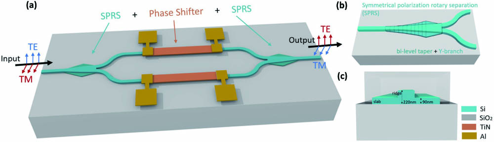
Silicon waveguides typically exhibit optical anisotropy, which leads to polarization correlation and single-polarization operations. This consequently creates a demand for polarization-control devices. This paper introduces a CMOS-compatible O-band reconfigurable TE/TM polarization rotator comprising two symmetrical polarization rotator–splitters and phase shifters. This configuration enables dynamic conversion of any linear polarization to its quadratic equivalent. Experimental results indicate that the reconfigurable polarization rotator exhibits an insertion loss of less than 1.5 dB. Furthermore, the bandwidth for a polarization extinction ratio beyond 15 dB exceeds 60 nm.
silicon-based optoelectronics polarization rotation polarization switch Chinese Optics Letters
2024, 22(1): 011303
1 西南技术物理研究所,四川 成都 610041
2 四川大学电子信息学院,四川 成都 610065
硅基光电子技术的发展可以将激光雷达系统发射模块和接收模块中分立的有源和无源器件集成在芯片上,使激光雷达体积更小、稳定性更强、成本更低,推动激光雷达在自动驾驶等领域的应用。首先,分析激光雷达的基本概念及测量原理。随后,根据扫描方式的不同,将硅基片上激光雷达分为面阵闪光、光学相控阵、透镜辅助光束转向和慢光光栅等4类,并分别对其技术特点和研究进展进行阐述。最后,对目前硅基片上激光雷达的发展趋势进行了总结和展望。
激光雷达 硅基光电子 面阵闪光 光学相控阵 透镜辅助光束转向 激光与光电子学进展
2023, 60(16): 1600002

Author Affiliations
Abstract
1 Peking University, State Key Laboratory of Advanced Optical Communication Systems and Networks, School of Electronics, Beijing, China
2 Chinese Academy of Sciences, Shanghai Institute of Optics and Fine Mechanics, Shanghai, China
Conventional electronic processors, which are the mainstream and almost invincible hardware for computation, are approaching their limits in both computational power and energy efficiency, especially in large-scale matrix computation. By combining electronic, photonic, and optoelectronic devices and circuits together, silicon-based optoelectronic matrix computation has been demonstrating great capabilities and feasibilities. Matrix computation is one of the few general-purpose computations that have the potential to exceed the computation performance of digital logic circuits in energy efficiency, computational power, and latency. Moreover, electronic processors also suffer from the tremendous energy consumption of the digital transceiver circuits during high-capacity data interconnections. We review the recent progress in photonic matrix computation, including matrix-vector multiplication, convolution, and multiply–accumulate operations in artificial neural networks, quantum information processing, combinatorial optimization, and compressed sensing, with particular attention paid to energy consumption. We also summarize the advantages of silicon-based optoelectronic matrix computation in data interconnections and photonic-electronic integration over conventional optical computing processors. Looking toward the future of silicon-based optoelectronic matrix computations, we believe that silicon-based optoelectronics is a promising and comprehensive platform for disruptively improving general-purpose matrix computation performance in the post-Moore’s law era.
silicon-based optoelectronics photonic matrix computation optical interconnections photonic-electronic integration Advanced Photonics
2022, 4(4): 044001
1 中国科学院半导体研究所 集成光电子学国家重点实验室,北京 100083
2 中国科学院大学 材料科学与光电技术学院,北京 100049
硅材料在1.1~8.5 μm有非常低的吸收损耗,因此硅基光电子学有望扩展到中红外波段。并且随着通信窗口扩展、气体分子检测、红外成像等应用需求的出现,硅基中红外波段器件研发工作的开展势在必行。在中红外波段硅基光电子器件中,硅基调制器有着举足轻重的地位:它是长波光通信链路中不可或缺的一环,还可以应用在片上传感系统中提高信噪比、实现光开关等功能。研究发现,相比于近红外波段,硅和锗材料在中红外波段有更强的自由载流子效应和热光效应,因此,基于硅基材料的中红外调制器具有独天得厚的优势。系统总结了中红外硅基调制器的发展趋势和研究现状,介绍了基于硅和锗材料的电光调制器以及热光调制器的工作原理和最新研究进展,最后对中红外硅基调制器进行了总结与展望。
中红外 硅基光电子 调制器 mid-infrared silicon-based optoelectronics modulator 红外与激光工程
2022, 51(3): 20220021
1 电子科技大学光电信息学院电子薄膜与集成器件国家重点实验室, 四川 成都 610054
2 电子科技大学核心电子材料与器件协同创新中心, 四川 成都 610054
随着光网络通信容量的高速增长, 将分立的光学器件集成化以减小器件尺寸、降低成本成为光电子器件发展的必然趋势。光子集成回路具有尺寸小、功耗低、质量轻等优点, 是解决未来宽带光网络能耗大、体积大、容量小等问题的关键技术。综述了基于多项目晶圆流片的规模化光子集成技术, 主要包括硅基光子集成技术、Ⅲ-V族磷化铟集成技术, 以及以氮化硅和二氧化硅多层波导结构为基础的TriPleX集成技术; 介绍了目前可以提供这3种多项目晶圆流片光子集成技术的代工平台以及利用这些代工平台实现的一些光子集成芯片, 并对这些平台的工艺参数进行了比较。
集成光学 光子集成器件 多项目晶圆流片 光子集成回路 硅基光电子学 磷化铟 激光与光电子学进展
2017, 54(5): 050001


