荧光成像技术探测熔石英元件亚表面缺陷  下载: 1246次
Subsurface Defects in Fused Silica Elements Detected by Fluorescence Imaging Technology
1 西南科技大学材料科学与工程学院, 四川 绵阳 621900
2 中国工程物理研究院激光聚变研究中心, 四川 绵阳 621900
图 & 表
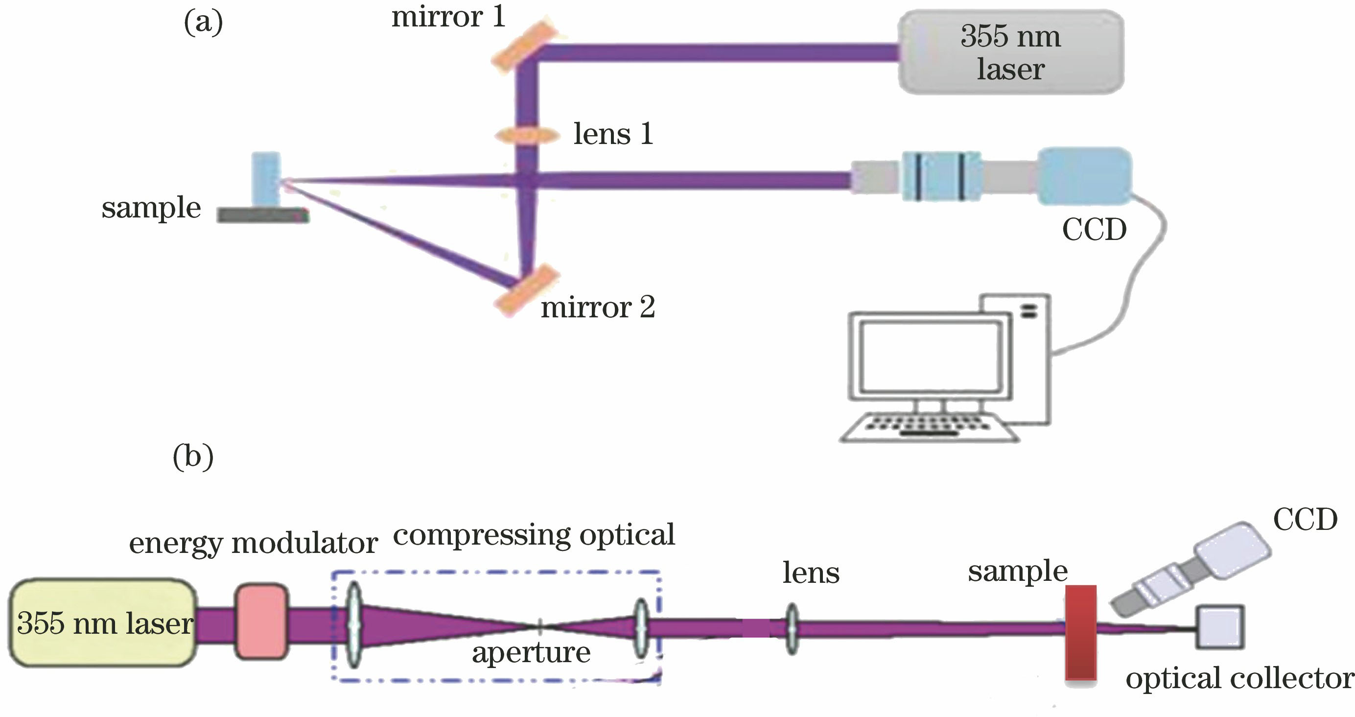
图 1. (a)荧光无损检测熔石英亚表面缺陷示意图;(b)光学元件的激光损伤测试光路示意图
Fig. 1. (a) Schematic of subsurface defect of fused silica in fluorescence non-destructive testing; (b) laser damage test optical path of optical elements
下载图片 查看原文
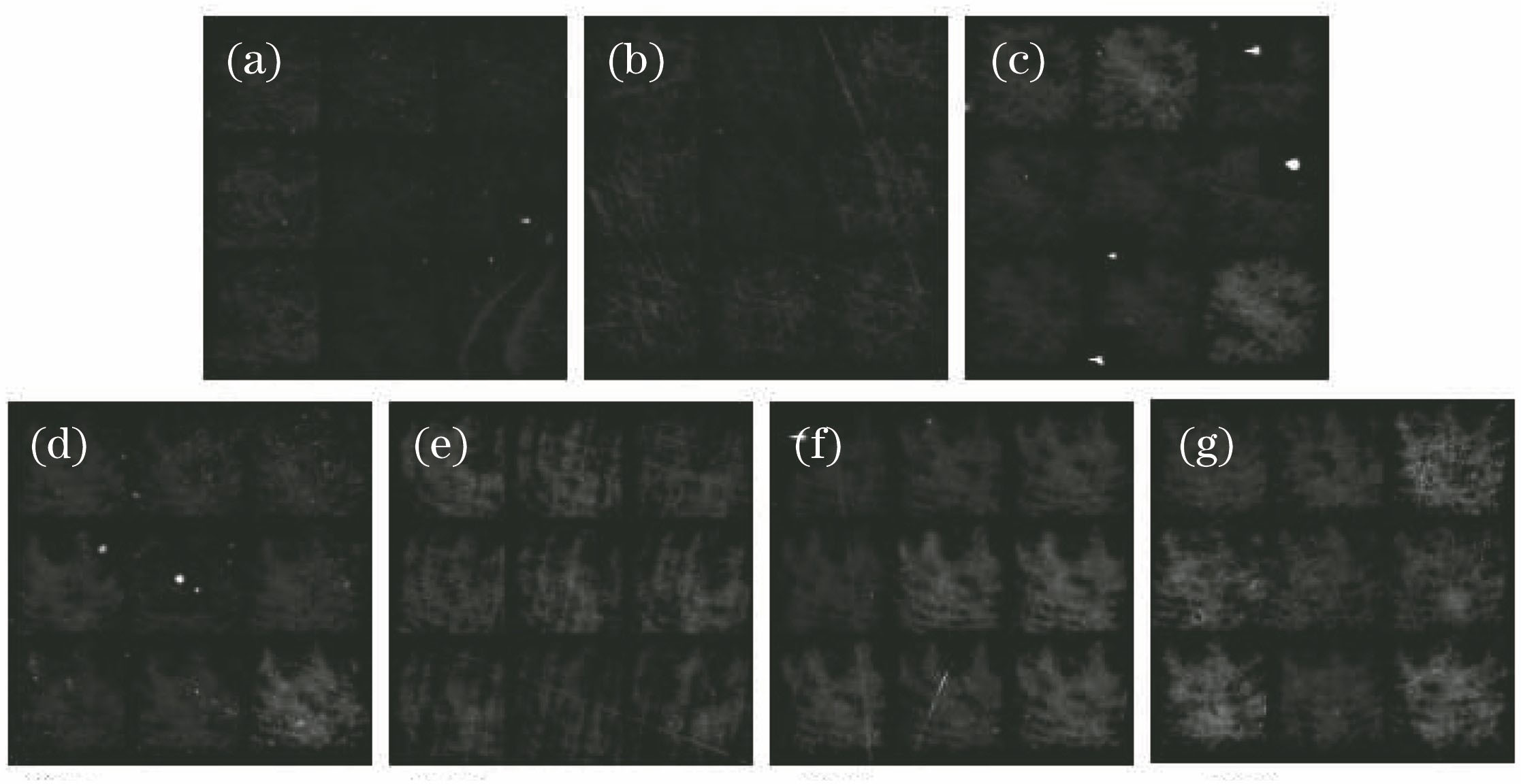
图 2. 熔石英元件亚表面缺陷的荧光图像。(a) Ort1;(b) Ort2;(c) Ort3;(d) Ort4;(e) Ort5;(f) Ort6;(g) Ort7
Fig. 2. Fluorescence images of subsurface defects of fused silica elements. (a) Ort1; (b) Ort2; (c) Ort3; (d) Ort4; (e) Ort5; (f) Ort6; (g) Ort7
下载图片 查看原文
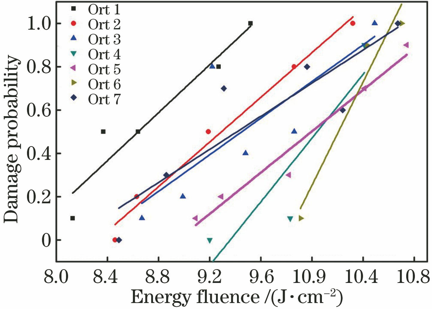
图 3. 熔石英光学元件的激光损伤概率与能量密度的关系曲线
Fig. 3. Curves of laser damage probability and energy density of fused silica optical elements
下载图片 查看原文
表 1各熔石英样品的粗糙度
Table1. Roughness of fused silica samples
| Elementnumber | Standard /(mm×mm) | RoughnessRq /nm |
|---|
| Ort1 | 50×30 | 1.247 | | Ort2 | 50×30 | 0.767 | | Ort3 | 50×30 | 0.647 | | Ort4 | 50×30 | 1.065 | | Ort5 | 50×50 | 1.077 | | Ort6 | 50×50 | 0.577 | | Ort7 | 50×50 | 0.913 |
|
查看原文
表 2荧光无损探测统计表
Table2. Fluorescence non-destructive detection statistics
| Elementnumber | Defectarea /μm | Area ratio ofdefects |
|---|
| Ort1 | 250 | 1.8×10⁻⁴ | | Ort2 | 102 | 4.0×10⁻⁵ | | Ort3 | 2779 | 1.1×10⁻³ | | Ort4 | 114 | 4.5×10⁻⁵ | | Ort5 | 110 | 4.3×10⁻⁵ | | Ort6 | 113 | 4.4×10⁻⁵ | | Ort7 | 162 | 6.3×10⁻⁵ |
|
查看原文
表 3不同熔石英样品的零概率损伤阈值
Table3. Zero-probability damage threshold for different fused silica sample
| Element number | Threshold /(J·cm-2) |
|---|
| Ort1 | 8.04 | | Ort2 | 9.79 | | Ort3 | 6.15 | | Ort4 | 8.62 | | Ort5 | 8.63 | | Ort6 | 8.95 | | Ort7 | 6.88 |
|
查看原文
李洪路, 刘红婕, 蒋晓东, 黄进, 曹林洪. 荧光成像技术探测熔石英元件亚表面缺陷[J]. 激光与光电子学进展, 2019, 56(1): 011004. Honglu Li, Hongjie Liu, Xiaodong Jiang, Jin Huang, Linhong Cao. Subsurface Defects in Fused Silica Elements Detected by Fluorescence Imaging Technology[J]. Laser & Optoelectronics Progress, 2019, 56(1): 011004.


 PDF全文
PDF全文

