
Author Affiliations
Abstract
1 State Key Laboratory on Integrated Optoelectronics, Institute of Semiconductors, Chinese Academy of Sciences, Beijing 100083, China
2 Center of Materials Science and Optoelectronics Engineering, University of Chinese Academy of Sciences, Beijing 100049, China
In this work, a two-step metal organic chemical vapor deposition (MOCVD) method was applied for growing β-Ga2O3 film on c-plane sapphire. Optimized buffer layer growth temperature (TB) was found at 700 °C and the β-Ga2O3 film with full width at half maximum (FWHM) of 0.66° was achieved. A metal?semiconductor?metal (MSM) solar-blind photodetector (PD) was fabricated based on the β-Ga2O3 film. Ultrahigh responsivity of 1422 A/W @ 254 nm and photo-to-dark current ratio (PDCR) of 106 at 10 V bias were obtained. The detectivity of 2.5 × 10¹⁵ Jones proved that the photodetector has outstanding performance in detecting weak signals. Moreover, the photodetector exhibited superior wavelength selectivity with rejection ratio (R250 nm/R400 nm) of 105. These results indicate that the two-step method is a promising approach for preparation of high-quality β-Ga2O3 films for high-performance solar-blind photodetectors.
MOCVD two-step growth β-Ga2O3 solar-blind photodetector responsivity Journal of Semiconductors
2024, 45(2): 022502
1 北京工业大学信息学部 光电子技术教育部重点实验室,北京 100124
2 长春理工大学 高功率半导体激光国家重点实验室,吉林 长春 130022
3 中国科学院 苏州纳米技术与纳米仿生研究所,江苏 苏州 215123
采用脉冲直流磁控溅射法在Si(100)衬底上制备了AlN/Mo/Sc0.2Al0.8N复合结构薄膜,在该结构上通过金属有机化学气相沉积(MOCVD)技术进行GaN薄膜的外延。使用原子力显微镜、高分辨X射线衍射、粉末X射线衍射、扫描电子显微镜和拉曼光谱研究了Mo插入层的厚度对Sc0.2Al0.8N缓冲层和GaN外延层晶体质量的影响,研究了Sc0.2Al0.8N缓冲层对Mo上生长的GaN外延层的影响。研究结果表明,Mo插入层的厚度是影响Sc0.2Al0.8N缓冲层和GaN外延层的重要因素,Sc0.2Al0.8N缓冲层对Mo上GaN晶体质量的提高具有重要意义。随Mo厚度的增加,Sc0.2Al0.8N缓冲层的表面粗糙度先减小后增大,GaN外延层的(002)面X射线衍射摇摆曲线半峰全宽先减小后增大。当Mo插入层厚度为400 nm时,GaN外延层的晶体质量最好,GaN(002)面的X射线衍射摇摆曲线半峰全宽为0.51°,由拉曼光谱计算得到的压应力483.09 MPa;直接在Mo上进行GaN的外延,GaN(002)面的X射线衍射摇摆曲线半峰全宽无法测得,说明在Mo上进行GaN的外延需要Sc0.2Al0.8N缓冲层。
GaN 金属有机化学气相沉积(MOCVD) ScAlN X射线衍射 GaN metal-organic chemical vapor deposition(MOCVD) ScAlN X-ray diffraction(XRD) 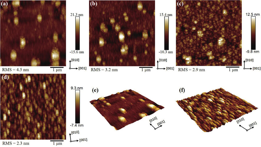
Author Affiliations
Abstract
1 School of Nano-Tech and Nano-Bionics, University of Science and Technology of China, Hefei 230026, China
2 Nanofabrication facility, Suzhou Institute of Nano-Tech and Nano-Bionics, Chinese Academy of Sciences, Suzhou 215123, China
3 Research Center of Laser Crystal, Shanghai Institute of Optics and Fine Mechanics, Chinese Academy of Sciences, Shanghai 201800, China
4 Hangzhou Institute of Optics and Fine Mechanics, Hangzhou 311421, China
Homoepitaxial growth of Si-doped β-Ga2O3 films on semi-insulating (100) β-Ga2O3 substrates by metalorganic chemical vapor deposition (MOCVD) is studied in this work. By appropriately optimizing the growth conditions, an increasing diffusion length of Ga adatoms is realized, suppressing 3D island growth patterns prevalent in (100) β-Ga2O3 films and optimizing the surface morphology with [010] oriented stripe features. The slightly Si-doped β-Ga2O3 film shows smooth and flat surface morphology with a root-mean-square roughness of 1.3 nm. Rocking curves of the (400) diffraction peak also demonstrate the high crystal quality of the Si-doped films. According to the capacitance–voltage characteristics, the effective net doping concentrations of the films are 5.41 × 10¹⁵ – 1.74 × 1020 cm−3. Hall measurements demonstrate a high electron mobility value of 51 cm2/(V·s), corresponding to a carrier concentration of 7.19 × 1018 cm−3 and a high activation efficiency of up to 61.5%. Transmission line model (TLM) measurement shows excellent Ohmic contacts and a low specific contact resistance of 1.29 × 10⁻⁴ Ω·cm2 for the Si-doped film, which is comparable to the Si-implanted film with a concentration of 5.0 × 1019 cm−3, confirming the effective Si doing in the MOCVD epitaxy.
homoepitaxial growth MOCVD Si-doping films high activation efficiency Ohmic contacts Journal of Semiconductors
2023, 44(6): 062801
1 中国科学技术大学纳米科学技术学院, 苏州 215123
2 中国科学院苏州纳米技术与纳米仿生研究所, 苏州 215123
3 苏州纳维科技有限公司, 苏州 215000
4 沈阳材料科学国家研究中心, 沈阳 110010
远程外延是一种用于生产单晶、独立式薄膜和结构的新兴技术, 该方法使用二维范德瓦耳斯材料作为半透明夹层, 实现外延生长及外延层在二维层界面的剥离。本文研究了在蓝宝石衬底上利用单层石墨烯作中间层异质远程外延GaN成核层、GaN薄膜。结果表明, GaN成核岛具有良好的取向, 通过参数调整, 可实现致密的GaN成核层。AFM和XRD测试结果证实, 与同样条件下蓝宝石衬底上直接生长的GaN薄膜相比, 石墨烯上异质远程外延得到的GaN薄膜具有更低的表面粗糙度和位错密度。
石墨烯 异质远程外延 表面粗糙度 位错密度 GaN GaN graphene MOCVD MOCVD remote heteroepitaxy surface roughness dislocation density
南京大学电子科学与工程学院, 江苏省光电功能材料重点实验室, 南京 210023
本文通过添加InGaN垫层, 利用金属有机物化学气相沉积(MOCVD)方法在GaN(0001)上外延生长了InN薄膜, 研究了InN薄膜的外延规律及光学性质。研究发现, 相对于GaN表面, 在InGaN垫层上可以获得更高质量的InN。通过在InGaN垫层中采用适当的In组分(在本工作中为In0.23Ga0.77N), 可以完全抑制InN生长过程中铟滴的形成, 获得的InN表面形貌连续平整。采用光学显微镜、高分辨率X射线衍射(HR-XRD)、透射电子显微镜(TEM)、光吸收和室温光致发光等方法研究了InN的晶体结构和光学性质。HR-XRD的ω和ω-2θ扫描显示, InGaN垫层消除了In滴的衍射信号, 并且ω扫描给出了150 nm的InN薄膜的(0002)半峰全宽为0.23°。TEM选区电子衍射发现, InN几乎是无应变的。室温下InN薄膜的光吸收和强光致发光结果表明, 所制备的InN薄膜能带隙约为0.74 eV。本文还初步研究了InN的异常激发依赖性的光致发光行为, 证明了InN材料的表面效应对辐射复合的强烈作用。
外延生长 应变 表面缺陷 光学性质 光致发光 InN InN MOCVD MOCVD epitaxial growth strain surface defect optical property photoluminescence
1 北京大学宽禁带半导体研究中心, 北京 100871
2 北京大学人工微结构和介观物理国家重点实验室, 北京 100871
3 教育部纳光电子前沿科学中心, 北京 100871
4 量子物质科学协同创新中心, 北京 100871
Si衬底因兼具大尺寸、低成本以及与现有CMOS工艺兼容等优势, 使Si衬底上GaN基射频(RF)电子材料和器件成为继功率电子器件之后下一个该领域关注的焦点。由于力学性质与低阻Si衬底不同, 高阻Si衬底上GaN基外延材料生长的应力控制和位错抑制问题仍然困难, 且严重的射频损耗问题限制着其在射频电子领域的应用。本文简要介绍了Si衬底上GaN基射频电子材料的研究现状和面临的挑战, 重点介绍了北京大学研究团队在高阻Si衬底上GaN基材料射频损耗的产生机理, 以及低位错密度、低射频损耗GaN的外延生长等方面的主要研究进展。最后对Si衬底上GaN基射频电子材料和器件的未来发展作了展望。
Si衬底上GaN 金属有机化合物化学气相沉积 应力 位错 射频损耗 GaN-on-Si MOCVD stress dislocation RF loss


