1 北京理工大学物理学院,北京 100081
2 昆明冶金高等专科学校建筑工程学院,云南昆明 650033
3 昆明物理研究所,云南昆明 650223
4 云南省先进光电材料与器件重点实验室,云南昆明 650223
GeTe基半导体的非晶态,.-GeTe相和.-GeTe相可以相互转换,且在一定条件下稳定存在。利用高浓度空穴掺杂改善 GeTe热电和铁电性能,以及非晶相和晶相间的巨大差异和快速切换,使其在热电、自旋器件、相变开关、相变存储等多个领域具有很大的应用前景。此外, GeTe具有窄光学带隙和高载流子迁移率,有望用于高性能红外光电探测,然而其在红外光电探测方面还处于初始阶段。本综述在详述其性质及在热电、相变等领域应用情况的基础上,根据 GeTe的光电性质,展望了其在红外光电探测领域方面的应用。
GeTe薄膜 物理性质 GeTe应用 光电探测器 GeTe thin films, physical properties, applications

Author Affiliations
Abstract
Photonic Device Physics Laboratory, Institute of Physics and Applied Physics, Yonsei University, 50 Yonsei-ro Seodaemun-gu, Seoul 120-749, South Korea
The denaturation of double-stranded deoxyribonucleic acid (ds-DNA) has been well known to break nucleobase bonds, resulting in single-stranded deoxyribonucleic acid (ss-DNA) in solutions, which can recombine to form ds-DNA in a reversible manner. We developed an efficient process to irreversibly maintain various DNA denaturation levels in thin solid films in order to investigate the impacts of the denaturation on the optical properties of DNA films. By adding NaOH in an aqueous solution of salmon testis DNA, we flexibly controlled the level of denaturation in the solution, which was then spin-coated on Si and silica substrates to irreversibly bind ss-DNAs in a thin solid film. The denaturation of DNA in thin solid films was experimentally confirmed by ultraviolet-visible and Fourier transform infrared spectroscopic investigations, whose level could be controlled by the NaOH content in the aqueous solution precursor. By this irreversible denaturation process, we developed a new method to flexibly vary the refractive index of DNA thin solid films in a wide range of Δn>0.02 in the visible to near-infrared range. Thermo-optic coefficients dn/dT of the films were also experimentally measured in the temperature range from 40°C to 90°C to confirm the significant impacts of denaturation. Detailed thin film processes and optical characterizations are discussed.
Biology Spectroscopy, ultraviolet Thin films, optical properties Photonics Research
2018, 6(9): 09000918

Author Affiliations
Abstract
1 College of Advanced Interdisciplinary Studies, National University of Defense Technology, Changsha 410073, China
2 State Key Laboratory of High Performance Computing, National University of Defense Technology, College of Computer, Changsha 410073, China
3 National Institute of Defense Technology Innovation, Academy of Military Sciences PLA China, Beijing 100010, China
4 e-mail: oscarwang2008@sina.com
Here, we used the micro P-scan method to investigate the saturated absorption (SA) of different layered continuous films. Through resonance excitation, first, we studied the influence of the second surface state (SS) on SA. The second SS resonance excitation () resulted in a free carrier cross section that was 4 orders of magnitude larger than usual. At the same time, we found that the fast relaxation process of the massless Dirac electrons is much shorter than that of electrons in bulk states. Moreover, the second SS excitation resonance reduced the saturation intensity. Second, we studied the effect of the thickness on the SA properties of materials. The results showed that the saturation intensity was positively correlated to the thickness, the same as the modulation depth, and the thicker the film was, the less the second SS would influence it. This work demonstrated that by using as a saturable absorber through changing the thickness or excitation wavelength, a controllable SA could be achieved.
Nonlinear optics, materials Thin films, optical properties Ultrafast nonlinear optics Photonics Research
2018, 6(10): 100000C8
Author Affiliations
Abstract
1 School of Physics, Raymond and Beverly Sackler Faculty of Exact Sciences, Tel Aviv University, Tel Aviv 69978, Israel
2 Center for Light-Matter Interaction, Tel Aviv University, Tel Aviv 69978, Israel
3 School of Chemistry, Raymond and Beverly Sackler Faculty of Exact Sciences, Tel Aviv University, Tel Aviv 69978, Israel
We show that Fourier-plane imaging in conjunction with the Kretschmann–Raether configuration can be used for measuring polariton dispersion with spatial discrimination of the sample, over the whole visible spectral range. We demonstrate the functionality of our design on several architectures, including plasmonic waveguides, and show that our new design enables the measurement of plasmonic dispersion curves of spatially inhomogeneous structures with features as small as 3 μm, in a single shot.
Surface plasmons Microscopy Waveguides Dispersion Spectroscopy, surface Thin films, optical properties Photonics Research
2018, 6(6): 06000653

Author Affiliations
Abstract
1 Changchun Observatory, NAO, Chinese Academy of Sciences, Changchun 130012, China
2 State Key Laboratory on Integrated Optoelectronics, College of Electronic Science & Engineering, Jilin University, Changchun 130012, China
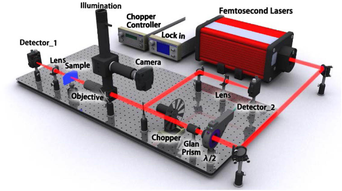
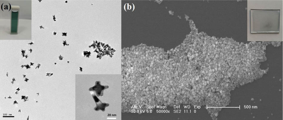
In this paper, we propose and demonstrate an all-fiber passively Q-switched erbium doped fiber laser (EDFL) by using gold nanostars (GNSs) as a saturable absorber (SA) for the first time, to the best of our knowledge. In comparison with other gold nanomorphologies, GNSs have multiple localized surface plasmon resonances, which means that they can be used to construct wideband ultrafast pulse lasers. By inserting the GNS SA into an EDFL cavity pumped by a 980 nm laser diode, a stable passively Q-switched laser at 1564.5 nm was achieved for a threshold pump power of 40 mW. By gradually increasing the pump power from 40 to 120 mW, the pulse duration decreases from 12.8 to 5.3 μs and the repetition rate increases from 10 to 17 kHz. Our results indicate that the GNSs are a promising SA for constructing pulse lasers.
Lasers, fiber Lasers, Q-switched Nanomaterials Thin films, optical properties Photonics Research
2018, 6(6): 06000549

Author Affiliations
Abstract
Science and Technology on Vacuum Technology and Physics Laboratory, Lanzhou Institute of Physics, Lanzhou 730001, China
Specimens of PbTe single film are deposited on Ge substrates by vacuum thermal evaporation. During the temperature range of 80–300 K, the transmittance of a PbTe film within 2–15 μm is measured every 20 K by the PerkinElmer Fourier transform infrared spectroscopy cryogenic testing system. Then, the relationship between the refractive index and wavelength within 7–12 μm at different temperatures is received by the full spectrum inversion method fitting. It can be seen that the relationship conforms to the Cauchy formula, which can be fitted. Then, the relationship between the refractive index of the PbTe film and the temperature/wavelength can be expressed as n(λ,T)=5.82840 0.00304T+4.61458×10 6T2+8.00280/λ2+0.21544/λ4, which is obtained by the fitting method based on the Cauchy formula. Finally, the designed value obtained by the formula and the measured spectrum are compared to verify the accuracy of the formula.
310.6860 Thin films, optical properties 120.4530 Optical constants 160.4670 Optical materials Chinese Optics Letters
2017, 15(4): 043101

Author Affiliations
Abstract
1 School of Optoelectronic Information, University of Electronic Science and Technology of China, Chengdu 610054, China
2 Institute of Optics and Electronics, Chinese Academy of Sciences, Chengdu 610209, China
The cavity ring-down (CRD) technique is adopted for simultaneously measuring s- and p-polarization reflectivity of highly reflective coatings without employing any polarization optics. As the s- and p-polarized light trapped in the ring-down cavity decay independently, with a randomly polarized light source the ring-down signal recorded by a photodetector presents a double-exponential waveform consisting of ring-down signals of both s- and p-polarized light. The s- and p-polarization reflectivity values of a test mirror are therefore simultaneously determined by fitting the recorded ring-down signal with a double-exponential function. The determined s- and p-polarization reflectivity of 30° and 45° angle of incidence mirrors are in good agreement with the reflectivity values measured with the conventional CRD technique employing a polarizer for polarization control.
310.0310 Thin films 310.6860 Thin films, optical properties 120.0120 Instrumentation, measurement, and metrology Chinese Optics Letters
2017, 15(5): 053101

Author Affiliations
Abstract
1 State Key Laboratory of Petroleum Resources and Prospecting, China University of Petroleum, Beijing 102249, China
2 Beijing Key Laboratory of Optical Detection Technology for Oil and Gas, China University of Petroleum, Beijing 102249, China
A lateral photovoltaic effect (LPE) is discovered in an LaTiO3+δ film epitaxially grown on a (100) SrTiO3 substrate. Under the illumination of a continuous 808 nm laser beam that is focused on the LaTiO3+δ film through the SrTiO3 substrate, the open-circuit photovoltage depends linearly on the illuminated position. The sensitivity of the LPE can be modified by the bias current. The LaTiO3+δ film shows a stable photoelectric property under the high pressure, up to 9 MPa. These results indicate that the LaTiO3+δ films can give rise to a potentially photoelectronic device for near-infrared position-sensitive detection in high-pressure environments.
310.6870 Thin films, other properties 230.5160 Photodetectors 040.5350 Photovoltaic Chinese Optics Letters
2016, 14(1): 013101

Author Affiliations
Abstract
1 Postdoctoral Mobile Research Station of the School of Electronic Engineering, Heilongjiang University, Harbin 150080, China
2 School of Applied Sciences, Harbin University of Science and Technology, Harbin 150080, China
3 Key Laboratory of Electronics Engineering, College of Heilongjiang Province, Heilongjiang University, Harbin 150080, China
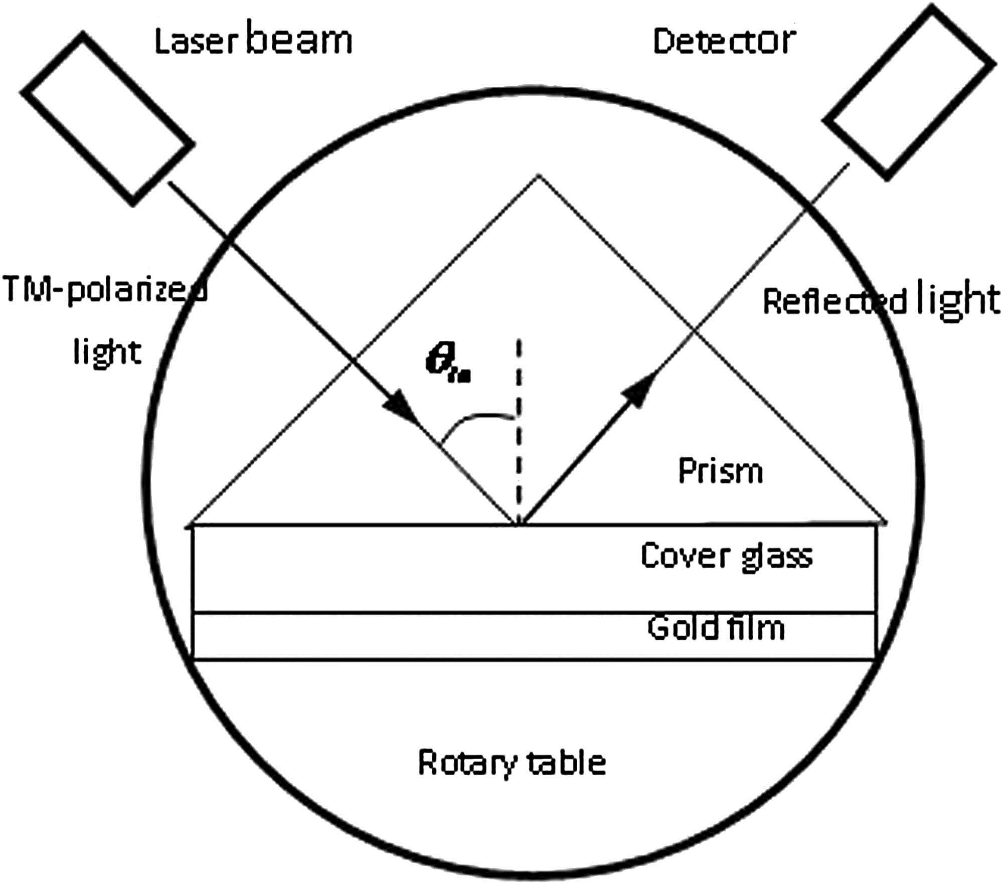
We experimentally investigate the effects of the surface roughness of gold thin films on the properties of surface plasmon resonance. By annealing at different temperatures, film samples with different surface morphologies are obtained. Specifically, due to the diffusion of the gold atoms towards the films’ surface, the surface root-mean-square roughness decreases with the increasing annealing temperature. Then, we measure the surface plasmon resonance of the samples. The results show that the resonance angle of the surface plasmon resonance is sensitive to the root-mean-square roughness, and it gradually decreases by reducing the surface root-mean-square roughness.
240.6680 Surface plasmons 310.6860 Thin films, optical properties Chinese Optics Letters
2016, 14(4): 042401

Author Affiliations
Abstract
State Key Laboratory of Modern Optical Instrumentation, College of Optical Science and Engineering, Zhejiang University, Hangzhou 310027, China
Silicon-rich oxide films with controllable optical constants and properties are deposited by the reactive magnetron sputtering method on a Si target. The O/Si atomic ratio x of SiOx is tuned from 0.12 to 1.84 by adjusting the oxygen flow rate, which is found to be a more effective way to obtain SiOx films compared with changing the oxygen content [O2/(Ar+O2) ratio]. The optical properties of SiOx films can be tuned from semiconductor to dielectric as a function of ratio x. The structures and components are also investigated by an x ray photoelectron spectroscopy analysis of the Si 2p core levels, the results of which exhibit that the structures of SiOx can be thoroughly described by the random bonding model.
160.4670 Optical materials 310.6860 Thin films, optical properties 310.1860 Deposition and fabrication Chinese Optics Letters
2016, 14(5): 051603


