Author Affiliations
Abstract
1 School of Computer Science and Engineering, Xi’an University of Technology, Xi’an, China
2 School of Information Science and Technology, Northwest University, Xi’an 710127, China
Optical molecular tomography (OMT) is a potential pre-clinical molecular imaging technique with applications in a variety of biomedical areas, which can provide non-invasive quantitative three-dimensional (3D) information regarding tumor distribution in living animals. The construction of optical transmission models and the application of reconstruction algorithms in traditional model-based reconstruction processes have affected the reconstruction results, resulting in problems such as low accuracy, poor robustness, and long-time consumption. Here, a gates joint locally connected network (GLCN) method is proposed by establishing the mapping relationship between the inside source distribution and the photon density on surface directly, thus avoiding the extra time consumption caused by iteration and the reconstruction errors caused by model inaccuracy. Moreover, gates module was composed of the concatenation and multiplication operators of three different gates. It was embedded into the network aiming at remembering input surface photon density over a period and allowing the network to capture neurons connected to the true source selectively by controlling three different gates. To evaluate the performance of the proposed method, numerical simulations were conducted, whose results demonstrated good performance in terms of reconstruction positioning accuracy and robustness.
Optical molecular tomography gates module positioning accuracy robustness Journal of Innovative Optical Health Sciences
2024, 17(3): 2350027

Author Affiliations
Abstract
1 Laboratory of Solid State Optoelectronics Information Technology, Institute of Semiconductors, Chinese Academy of Sciences, Beijing 100083, China
2 College of Materials Science and Opto-Electronic Technology, University of Chinese Academy of Sciences, Beijing 101804, China
3 School of Physics Science and Technology, Xinjiang University, Urumqi 830046, China
4 School of New Energy and Electronics, Yancheng Teachers University, Yancheng 224002, China
5 Key Laboratory of Optoelectronic Materials and Devices, Institute of Semiconductors, Chinese Academy of Sciences, Beijing 100083, China
Ex situ characterization techniques in molecular beam epitaxy (MBE) have inherent limitations, such as being prone to sample contamination and unstable surfaces during sample transfer from the MBE chamber. In recent years, the need for improved accuracy and reliability in measurement has driven the increasing adoption of in situ characterization techniques. These techniques, such as reflection high-energy electron diffraction, scanning tunneling microscopy, and X-ray photoelectron spectroscopy, allow direct observation of film growth processes in real time without exposing the sample to air, hence offering insights into the growth mechanisms of epitaxial films with controlled properties. By combining multiple in situ characterization techniques with MBE, researchers can better understand film growth processes, realizing novel materials with customized properties and extensive applications. This review aims to overview the benefits and achievements of in situ characterization techniques in MBE and their applications for material science research. In addition, through further analysis of these techniques regarding their challenges and potential solutions, particularly highlighting the assistance of machine learning to correlate in situ characterization with other material information, we hope to provide a guideline for future efforts in the development of novel monitoring and control schemes for MBE growth processes with improved material properties.
epitaxial growth thin film in situ characterization molecular beam epitaxy (MBE) Journal of Semiconductors
2024, 45(3): 031301
Author Affiliations
Abstract
State Research Institute Center for Physical Sciences and Technology, Savanorių ave. 231, LT-02300 Vilnius, Lithuania
We introduce a novel method to create mid-infrared (MIR) thermal emitters using fully epitaxial, metal-free structures. Through the strategic use of epsilon-near-zero (ENZ) thin films in InAs layers, we achieve a narrow-band, wide-angle, and p-polarized thermal emission spectra. This approach, employing molecular beam epitaxy, circumvents the complexities associated with current layered structures and yields temperature-resistant emission wavelengths. Our findings contribute a promising route towards simpler, more efficient MIR optoelectronic devices.
epsilon-near-zero thermal emitters indium arsenide LWIR (long wave infraRed) molecular beam epitaxy Journal of Semiconductors
2024, 45(2): 022101
1 咸阳师范学院离子束与光物理实验室,陕西 咸阳 712000
2 西安交通大学物理学院,陕西 西安 710049
3 中国科学院近代物理研究所,甘肃 兰州 730000
用动能为1360 keV的129Xeq+(q=17,20,23,25,27)高电荷态离子分别入射到金属Al和Ti固体靶表面,测量高电荷离子与表面相互作用过程中离子俘获表面电子完成中性化所形成的激发态Xe原子和低电离态Xe离子退激辐射的近红外光谱线(800~1700 nm),以及靶原子被离化激发、退激辐射的光谱线。实验结果表明:高电荷态离子入射金属表面的过程中,携带的势能在飞秒量级的时间内沉积到靶表面,使靶原子离化激发,较强的库仑势能可使靶原子形成高离化态和复杂的电子组态、退激辐射光谱线。随着入射离子的电荷态增加,测量谱线的强度增大,该变化趋势与入射离子的势能随电荷增加的变化趋势大体一致,说明经典过垒模型在近玻尔速度能区是成立的。
原子与分子物理学 高电荷态离子 经典过垒模型 禁戒跃迁 近红外光谱
强激光与粒子束
2024, 36(1): 016003
浙江大学光电科学与工程学院极端光学技术与仪器全国重点实验室,浙江 杭州 310027
生命体是由大量有机排列的分子组成的,其结构不仅与分子的位置分布有关,还与分子的排列方式和空间取向有关。偏振荧光显微成像技术利用荧光的偏振特性,能够对生物结构的分子取向进行观测和成像,进而从分子层面揭示生命活动的功能和代谢信息,有力推动了生物医学相关领域的研究和发展。本文从偏振荧光成像原理出发,对目前存在的多种偏振荧光显微成像技术进行原理介绍和现状分析,列举了其在生物医学领域的相关应用,讨论了其发展趋势及前景,旨在为该领域的科研人员了解偏振荧光显微成像技术提供参考。
偏振荧光显微 偏振调制 分子取向 空间角度传递 超分辨 激光与光电子学进展
2024, 61(6): 0618011
Author Affiliations
Abstract
1 School of Nano-Tech and Nano-Bionics, University of Science and Technology of China, Hefei 230026, China
2 Suzhou Institute of Nano-Tech and Nano-Bionics, Chinese Academy of Sciences, Suzhou 215123, China
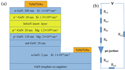
The InGaN films and GaN/InGaN/GaN tunnel junctions (TJs) were grown on GaN templates with plasma-assisted molecular beam epitaxy. As the In content increases, the quality of InGaN films grown on GaN templates decreases and the surface roughness of the samples increases. V-pits and trench defects were not found in the AFM images. p++-GaN/InGaN/n++-GaN TJs were investigated for various In content, InGaN thicknesses and doping concentration in the InGaN insert layer. The InGaN insert layer can promote good interband tunneling in GaN/InGaN/GaN TJ and significantly reduce operating voltage when doping is sufficiently high. The current density increases with increasing In content for the 3 nm InGaN insert layer, which is achieved by reducing the depletion zone width and the height of the potential barrier. At a forward current density of 500 A/cm2, the measured voltage was 4.31 V and the differential resistance was measured to be 3.75 × 10?3 Ω·cm2 for the device with a 3 nm p++-In0.35Ga0.65N insert layer. When the thickness of the In0.35Ga0.65N layer is closer to the “balanced” thickness, the TJ current density is higher. If the thickness is too high or too low, the width of the depletion zone will increase and the current density will decrease. The undoped InGaN layer has a better performance than n-type doping in the TJ. Polarization-engineered tunnel junctions can enhance the functionality and performance of electronic and optoelectronic devices.
GaN/InGaN/GaN tunnel junctions polarization-engineering molecular beam epitaxy Journal of Semiconductors
2024, 45(1): 012503
中国矿业大学信息与控制工程学院,江苏 徐州 221116
提出了一种基于电磁诱导透明(EIT)的多功能偏振无关超表面,其基础结构由1个金属十字结构和4个方环结构组成,并引入了可调控材料硅(Si)以及二氧化钒(VO2),以实现温光双控。利用模拟计算和理论模型分析得到了基础结构作为双明模间接耦合形成EIT透明窗口的结论。由于EIT以及可调控材料的特性,本设计可以在分子传感、可控慢光以及双通道温光双控开关等领域实现应用,并且具有优异的性能。该结构对蔗糖溶液的传感灵敏度为97.6 GHz/(kg/m3),在分子检测领域展示出了巨大潜力。该结构实现了对慢光效应的可选择控制。依据EIT的作用机理,提出了利用可调控材料改变结构谐振进而控制电磁响应的设计思路,并实现了一种双通道温光双控开关,为今后的EIT超表面设计提供了参考。
表面光学 超表面 可调控材料 分子传感 慢光效应 温光双控开关

Author Affiliations
Abstract
1 State Key Laboratory of Superlattices and Microstructures, Institute of Semiconductors, Chinese Academy of Sciences, Beijing 100083, China
2 Center of Materials Science and Optoelectronics Engineering, University of Chinese Academy of Sciences, Beijing 100190, China
(Ga,Fe)Sb is a promising magnetic semiconductor (MS) for spintronic applications because its Curie temperature (TC) is above 300 K when the Fe concentration is higher than 20%. However, the anisotropy constant Ku of (Ga,Fe)Sb is below 7.6 × 10³ erg/cm3 when Fe concentration is lower than 30%, which is one order of magnitude lower than that of (Ga,Mn)As. To address this issue, we grew Ga1-x-yFexNiySb films with almost the same x (≈24%) and different y to characterize their magnetic and electrical transport properties. We found that the magnetic anisotropy of Ga0.76-yFe0.24NiySb can be enhanced by increasing y, in which Ku is negligible at y = 1.7% but increases to 3.8 × 10⁵ erg/cm3 at y = 6.1% (TC = 354 K). In addition, the hole mobility (μ) of Ga1-x-yFexNiySb reaches 31.3 cm2/(V?s) at x = 23.7%, y = 1.7% (TC = 319 K), which is much higher than the mobility of Ga1-xFexSb at x = 25.2% (μ = 6.2 cm2/(V?s)). Our results provide useful information for enhancing the magnetic anisotropy and hole mobility of (Ga,Fe)Sb by using Ni co-doping.
magnetic semiconductor molecular beam epitaxy Fe-Ni co-doping magnetic anisotropy hole mobility Journal of Semiconductors
2024, 45(1): 012101
1 吉林大学白求恩第一医院核医学科,吉林 长春 130021
2 空军航空大学航空基础学院,吉林 长春 130022
3 空军航空大学作战勤务学院,吉林 长春 130022
4 吉林大学原子与分子物理研究所,吉林 长春 130012
针对飞秒脉冲激光诱导击穿光谱(fs-LIBS)中Al靶温度对AlO分子光谱的影响进行了实验研究。通过测量AlO分子的光谱强度和振动温度,发现Al靶温度对fs-LIBS技术中AlO分子的光谱特性有显著的影响。研究结果表明,提高靶材温度能有效增强fs-LIBS中AlO分子的光谱信号强度,并提高分子的振动温度和寿命。此外,时间分辨光谱分析结果还揭示出在高Al靶温度条件下,AlO分子的辐射寿命较长,光谱信号强度较强。这意味着在高温下,分子能够停留更长的时间,增加了光谱信号的持续时间。通过调控飞秒激光能量和靶材温度,可以获得更强的分子发射和光谱信号,从而实现更高的灵敏度和准确性。研究结果为fs-LIBS技术中样品温度对分子光谱的调控机制研究提供了实验数据。
光谱学 激光诱导击穿光谱 飞秒激光 分子光谱 样品温度 AlO


