Journal of Semiconductors, 2023, 44 (8): 082001, Published Online: Sep. 21, 2023  

Pressure manipulation of ultrafast carrier dynamics in monolayer WS2

Author Affiliations
1 New Materials and New Energies, Shen Zhen Technology University, Shenzhen 518118, China
2 Analysis and Testing Center, Shen Zhen Technology University, Shenzhen 518118, China
Abstract
Two-dimensional transition metal dichalcogenides (TMDs) have intriguing physic properties and offer an exciting platform to explore many features that are important for future devices. In this work, we synthesized monolayer WS2 as an example to study the optical response with hydrostatic pressure. The Raman results show a continuous tuning of the lattice vibrations that is induced by hydrostatic pressure. We further demonstrate an efficient pressure-induced change of the band structure and carrier dynamics via transient absorption measurements. We found that two time constants can be attributed to the capture process of two kinds of defect states, with the pressure increasing from 0.55 GPa to 2.91 GPa, both of capture processes were accelerated, and there is an inflection point within the pressure range of 1.56 GPa to 1.89 GPa. Our findings provide valuable information for the design of future optoelectronic devices.

1 Introduction

Two-dimensional transition metal dichalcogenides (TMDs) have rich electrical, optical, chemical properties, and their bandwidth ranges from visible to infrared. Owing to the excellent mechanical, optical, and electrical properties, TMDs are suitable materials for sensors, catalysts, storage batteries, optoelectronic devices, and excitonic devices[14]. Monolayer WS2 is an atomically thin two-dimensional material, which is a sandwich structure, and is composed of a single layer transition metal tungsten (W) and two layers of chalcogen (S)[5, 6].

One key issue in harnessing novel properties of TMDs is to understand and control the carrier dynamic processes. Because the performance of TMDs-based photoelectric devices are closely related to the carrier dynamics process, effective and continuous tuning of carrier dynamics in TMDs is highly desired. Hydrostatic pressure is pure and clean because no additional impurities are introduced by the hydrostatic pressure of the diamond anvil cell (DAC). Recent reports have indicated that the optoelectronic properties of TMDs can be effectively tuned via hydrostatic pressure, such as the interaction of interlayer, material structure, carrier density, and conductivity[713]. The semiconductor to metallic phase transition in bulk WS2 is caused by hydrostatic pressure[14, 15]. In contrast, there are few studies on the carrier recombination of monolayer TMDs under pressure. Thus, it is of great value to develop an understanding of the carrier dynamics in TMDs with pressure.

Here, monolayer WS2 is used as a sample to study the carrier dynamics via transient absorption measurements. Our results demonstrate a pressure-induced blue shift of the A-exciton resonance, and two kinds of carrier capture processes of defect states can be continuously tuned by hydrostatic pressure. This study provides basic information for understanding the dynamics of carrier in TMDs, which may be useful in the design of new photoelectric devices that are based on TMDs.

2 Synthesis and material characterization

The WS2 monolayers were grown by CVD technique at 800 °C for 20 min onto SiO2/Si, as shown in Fig. 1. Sulfur powder and tungsten trioxide powder with a purity of 99.9% were used as source materials for experimental preparation of samples. Meanwhile, 0.2-g sulfur powder was placed on the crucible in the first temperature zone, and 0.1-g tungsten trioxide powder was placed on the crucible in the second temperature zone. Furthermore, 40 sccm (cubic centimeters per minute) Ar and 5 sccm H2 was used as the carrier gas to transfer the evaporated sulfur vapor to the substrate. We raised the temperature of furnace 1 from 25 °C to 200 °C for 1 h, and the temperature of furnace 2 from 25 °C to 800 °C, and maintained the temperature for 20 min. The S powder is gasified in the low temperature area, transported to the high temperature area by the carrier gas, and reacts with the gasified WO3 on the substrate to generate WS2. The whole CVD equipment was then naturally cooled down to room temperature.

Fig. 1. (Color online) Experimental setup of the CVD growth of monolayer WS2 sample.

下载图片 查看所有图片

The size of the sample prepared by CVD method can reach 40 μm, as shown in Fig. 2(a). The Raman spectra and photoluminescence (PL) spectra of the sample are shown in Figs. 2(c) and 2(d), respectively. The PL peak of the sample is centered at 615 nm. The Raman peaks of the sample is centered at 350 cm−1 and 418 cm−1, which represents the E2g1 and A1g peaks of WS2, respectively. The difference between the E2g1 and A1g peaks is 68 cm−1, which is in accord with the characteristics of single layer WS2[16]. The schematics of these two Raman modes E12g and A1g are shown in Fig. 2(b), the A1g mode of monolayer WS2 originates from the transverse out-of-plane relative vibration between sulfur atoms in the interlayer, while the E12g mode originates from the in-plane longitudinal vibration of tungsten and sulfur atoms in opposite directions. Therefore, E12g mode vibration is sensitive to the length of W−S bond. The PL peak of the monolayer WS2 lies at 615 nm (2.02 eV), which indicates that the valence band top and the conduction band bottom of the monolayer WS2 are located at the transition point, which is a direct bandgap[11]. The AFM image show that the thickness of our monolayer WS2 sample is 0.8 nm, which is shown in Fig. 2(e) and Fig. 2(f).
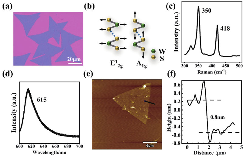
Fig. 2. (Color online) The characterization of monolayer WS2. (a) Optical image of a monolayer WS2. (b) Schematics of Raman modes of E2g1 and A1g. (c) Raman spectra of monolayer WS2 sample. (d) PL spectra of monolayer WS2 sample. (e) AFM image of monolayer WS2 sample. (f) Height image intensity profile along the black line in (e).

下载图片 查看所有图片

The monolayer WS2 was peeled from the substrate with the PVP/PVA adsorption transfer method. The pressure device used in this experiment is a four-column DAC, and the size of diamond plane is 300 μm. The T301 gasket was pre-pressed to 50 μm, and a hole with a diameter of 100 μm was punched in the center with a laser. Silicone oil was chosen as a pressure transmission medium. The silicone oil, the monolayer WS2 sample, and a 10 μm ruby were placed in the hole. The DAC device was used to gradually increase the pressure of the monolayer WS2 heterostructure to 2.91 GPa from 0 GPa, and the direction in which the pressure applied is perpendicular to the plane of the monolayer WS2 sample.

3 Results and discussion

Raman measurements were performed to study the lattice vibration of the monolayer WS2 sample when pressurized in the DAC[17] and the pressure transmission medium (PTM) is silicone oil. The evolutions of Raman spectra show a clear pressure-induced changeover, the feature at 350 cm−1 and 418 cm−1 (E12g and A1g modes of monolayer WS2) blue shift as the pressure increases (as shown in Fig. 3(a)), which is similar to other layered materials[18, 19]. The Raman peak as a function of pressure is shown in Fig. 3(b), and there are two linear increases at a rate of 3.1 cm−1GPa−1 (A1g) and 1.8 cm−1GPa−1 (E12g), respectively. The A1g modes are more sensitive to pressure than that of the E12g modes, which may be the reason why the out-of-plane motion of S−S bonds of A1g modes is more sensitive than the in-plane motion of the W−S bonds of the E12g modes under pressure. Therefore, the out-of-plane compression is more favorable than in plane compression under pressure[20, 21].
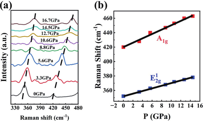
Fig. 3. (Color online) Pressure-induced Raman vibration in monolayer WS2. (a) Evolution of the Raman spectrum with pressure for monolayer WS2 sample. (b) Raman vibrations of monolayer WS2 as a function of pressure.

下载图片 查看所有图片

The PL spectra of monolayer WS2 with different pressures were measured, as shown in Fig. 4(a). The PL peaks have a blue shift with an increase in pressure from 0 GPa to 2.91 GPa. The PL peaks as a function of pressure are shown in Fig. 4(b), and there is a linear increase at a rate of −2.1 nm−1GPa−1. The change of the bandgap can be attributed to the enhanced quantum confinement effect caused by the pressure.
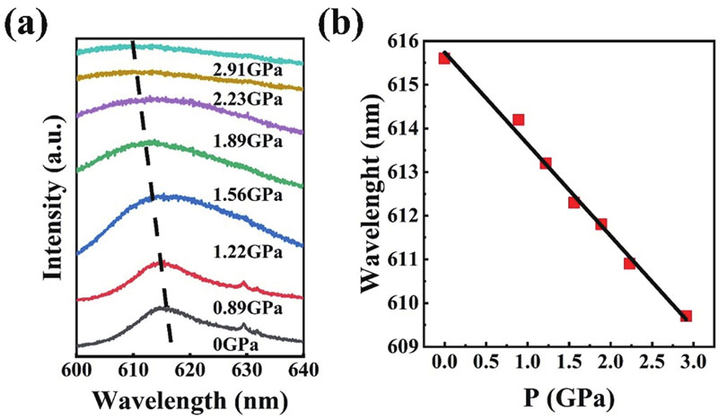
Fig. 4. (Color online) (a) Evolution of the PL spectra of monolayer WS2 sample with pressures. (b) PL peaks of monolayer WS2 as a function of pressure.

下载图片 查看所有图片

The transient absorption (TA) spectra of monolayer WS2 with different pressures were measured to gain more insight of the carrier dynamics process (as shown in Fig. 5(a)). For monolayer WS2, the applied pump wavelength is 400 nm and the pump peak fluence is 10 μJ/cm2. All of the samples were measured at room temperature.
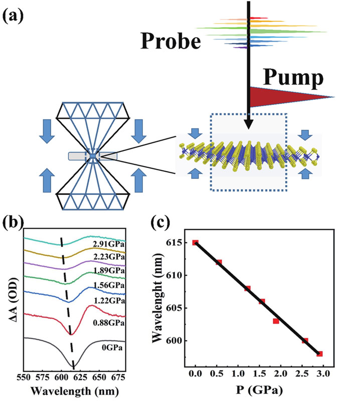
Fig. 5. (Color online) (a) Schematic of material structure and TA measurements of monolayer WS2 in the DAC. (b) Evolution of TA spectra of monolayer WS2 under pressure from 0.30 to 3.25 Gpa. (c) A exciton peaks as a function of pressures.

下载图片 查看所有图片

The absorption peaks of monolayered WS2 lies at 605−615 nm, which can be assigned to the A exciton resonance of WS2, and the photo-induced bleaching signals indicate that the corresponding energy states are occupied by photo-induced carriers. The TA spectra traces of A excitons are shown in Fig. 5(b) as the pressure ranged from 0.55 to 2.91 GPa at a time delay of 3 ps. A blue shift of the A exciton and the decrease of the intensity is observed with the increase of pressure. As shown in Fig. 5(c), the peaks of photo-induced signals with different pressures can be linearly fitted with a slope of −5.93 nm/GPa. These features might be caused by the pressure-induced enlargement of the bandgap of TMDs[2225].

The representative TA signals of A excitons with different pressures were recorded, as shown in Fig. 6. The decay curve can be well fitted as ΔA=A1eτ1+A2eτ2 with two time constants. Because the vacancies of atoms and grain boundary dislocations are common in TMDs, the capture process of shallow and deep defects states may give rise to the time constants τ1 and τ2[2628].
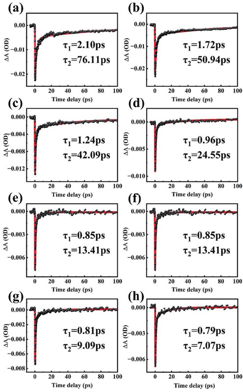
Fig. 6. (Color online) The transient absorption signals of monolayer WS2 with different pressures: (a) 0.55 GPa; (b) 0.89 Gpa; (c) 1.22 Gpa; (d) 1.56 GPa; (e) 1.89 GPa; (f) 2.23 Gpa; (g) 2.56 Gpa; (h) 2.91 GPa. The red lines are fitting.

下载图片 查看所有图片

It should be noted that the carrier capture process gets faster when increasing the pressure from 0.55 to 2.91 GPa, and can be divided into two distinct regions according to the slope variation of time constants upon compression, as shown in Fig. 7. For 0.55 GPa < P < 1.56 GPa, τ1 changes with pressure at a rate of −1.12 ps/GPa and τ2 declines with pressure at a rate of −51.78 ps/GPa. When the pressure is above 1.89 GPa, τ1 shows a decline shift at a rate of −0.07 ps/GPa and that of τ2 decreases to −6.38 ps/GPa.
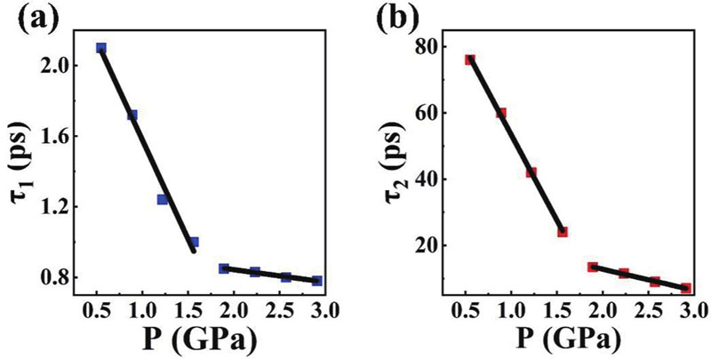
Fig. 7. (Color online) The time constants (a) τ1 and (b) τ2 of A exciton as a function of pressure.

下载图片 查看所有图片

For monolayer TMDs, the time constants τ1 and τ2 can be assigned to the carrier trapping process of the shallow and deep defect state with different capture rates. Considering the reduced dielectric screening effect and strong quantum confinement effect of TMDs, the Auger type dynamic process can be realized at low carrier densities. The τ1 and τ2 may be caused by Auger type carrier capture process of defect states, which means the electrons or holes in exciton states are captured by defect states by transferring the excess energy to other electrons and holes to satisfy the energy conservation law[29, 30]. According to this model, the quantum confinement effect may be enhanced by increasing the pressure, and the carriers are much easier to collide with other carriers. This feature means that the carriers are easier to release the excess energy to other electrons or holes, and this is beneficial for the Auger type carrier trapping process[3133]. However, there is a different model that can explain the pressure-induced acceleration of the carrier capture process—the pressure can shorten the W−S bond in the monolayer WS2, and enhance the vibration between W and S atoms, which can increase phonon energy and be confirmed by the above Raman results. This feature is conducive to meet the requirements of energy and momentum conservation in the capturing process[20, 21].

At around 1.56−1.89 GPa, a turning point appears and changes the time constants of two decay process with the decrease of pressure, which may result from the pressure induced changeover of the electronic structure. Both of the transient components are fully recovered when the pressure is released. Thus, the results clearly demonstrate that the band structure and carrier dynamics processes of monolayer WS2 can be accurately manipulated by hydrostatic pressure.

4 Conclusions

In summary, we have synthesized a sample monolayer WS2 to study the optical response of the sample with pressure via Raman spectroscopy and transient absorption spectroscopy. We found that hydrostatic pressure can be an efficient method to tune the lattice vibrations. The transition spectra were analyzed by tracking the energy shift and carrier dynamics of A exciton with different pressures. The results demonstrate the efficient tuning of band structure and photo-induced carrier recombination processes by pressure engineering. Our findings provide the basic information for understanding carrier dynamics in atomically thin TMDs under external strain.

References

[1] SharmaIMehtaB REnhanced charge separation at 2D MoS2/ZnS heterojunction: KPFM based study of interface photovoltageAppl Phys Lett201711006160210.1063/1.4975779

[2] RossR TNozikA JEfficiency of hot-carrier solar energy convertersJ Appl Phys198253381310.1063/1.331124

[3] LiuH SHanN NZhaoJ JAtomistic insight into the oxidation of monolayer transition metal dichalcogenides: From structures to electronic propertiesRSC Adv201551757210.1039/C4RA17320A

[4] ParzingerEMillerBBlaschkeBet alPhotocatalytic stability of single- and few-layer MoS2ACS Nano201591130210.1021/acsnano.5b04979

[5] WangQ HKalantar-ZadehKKisAet alElectronics and optoelectronics of two-dimensional transition metal dichalcogenidesNat Nanotechnol2012769910.1038/nnano.2012.193

[6] GeimA KGrigorievaI VVan der Waals heterostructuresNature201349941910.1038/nature12385

[7] YinZ YLiHLiHet alSingle-layer MoS2 phototransistorsACS Nano201267410.1021/nn2024557

[8] ChoiWChoM YKonarAet alHigh-detectivity multilayer MoS2 phototransistors with spectral response from ultraviolet to infraredAdv Mater201224583210.1002/adma.201201909

[9] HeY MYangYZhangZ Het alStrain-induced electronic structure changes in stacked van der Waals heterostructuresNano Lett201616331410.1021/acs.nanolett.6b00932

[10] ChenMXiaJ AZhouJ Det alACS Nano201711919110.1021/acsnano.7b04158

[11] NayakA PYuanZCaoB Xet alPressure-modulated conductivity, carrier density, and mobility of multilayered tungsten disulfideACS Nano20159911710.1021/acsnano.5b03295

[12] ZhuZ YChengY CSchwingenschlöglUGiant spin-orbit-induced spin splitting in two-dimensional transition-metal dichalcogenide semiconductorsPhys Rev B20118415340210.1103/PhysRevB.84.153402

[13] YeZ LCaoTO’BrienKet alProbing excitonic dark states in single-layer tungsten disulphideNature201451321410.1038/nature13734

[14] SelviEMaY ZAksoyRet alHigh pressure X-ray diffraction study of tungsten disulfideJ Phys Chem Solids200667218310.1016/j.jpcs.2006.05.008

[15] HangyoMNakashimaS IMitsuishiARaman spectroscopic studies of MX2-type layered compoundsFerroelectrics19835215110.1080/00150198308208248

[16] Ramakrishna MatteH S SGomathiAMannaAet alMoS2 and WS2 analogues of grapheneAngew Chem Int Ed201049405910.1002/anie.201000009

[17] DuwalSYooC SShear-induced isostructural phase transition and metallization of layered tungsten disulfide under nonhydrostatic compressionJ Phys Chem C2016120510110.1021/acs.jpcc.5b10759

[18] LivnehTStererEResonant Raman scattering at exciton states tuned by pressure and temperature in 2H-MoS2Phys Rev B20108119520910.1103/PhysRevB.81.195209

[19] NicolleJMachonDPoncharalPet alPressure-mediated doping in grapheneNano Lett201111356410.1021/nl201243c

[20] ChengX RLiY YShangJ Met alThickness-dependent phase transition and optical behavior of MoS2 films under high pressureNano Res20181185510.1007/s12274-017-1696-y

[21] ChiZ HZhaoX MZhangH Det alPressure-induced metallization of molybdenum disulfidePhys Rev Lett201411303680210.1103/PhysRevLett.113.036802

[22] NayakA PPandeyTVoiryDet alPressure-dependent optical and vibrational properties of monolayer molybdenum disulfideNano Lett20151534610.1021/nl5036397

[23] DouX MDingKJiangD Set alTuning and identification of interband transitions in monolayer and bilayer molybdenum disulfide using hydrostatic pressureACS Nano20148745810.1021/nn502717d

[24] LiF FYanY LHanBet alPressure confinement effect in MoS2 monolayersNanoscale20157907510.1039/C5NR00580A

[25] XiaJYanJ XWangZ Het alStrong coupling and pressure engineering in WSe2–MoSe2 heterobilayersNat Phys2020179210.1038/s41567-020-1005-7

[26] WangH NZhangC JRanaFUltrafast dynamics of defect-assisted electron–hole recombination in monolayer MoS2Nano Lett20151533910.1021/nl503636c

[27] CunninghamP DMcCrearyK MHanbickiA Tet alCharge trapping and exciton dynamics in large-area CVD grown MoS2J Phys Chem C2016120581910.1021/acs.jpcc.6b00647

[28] WangM SLiWScarabelliLet alPlasmon-trion and plasmon-exciton resonance energy transfer from a single plasmonic nanoparticle to monolayer MoS2Nanoscale201791394710.1039/C7NR03909C

[29] RuppertCChernikovAHillH Met alThe role of electronic and phononic excitation in the optical response of monolayer WS2 after ultrafast excitationNano Lett20171764410.1021/acs.nanolett.6b03513

[30] LiY ZShiJ AMiYet alUltrafast carrier dynamics in two-dimensional transition metal dichalcogenidesJ Mater Chem C20197430410.1039/C8TC06343E

[31] AhnCLimHSynthesis of monolayer 2D MoS2 quantum dots and nanomesh films by inorganic molecular chemical vapor deposition for quantum confinement effect controlBull Korean Chem Soc202243118410.1002/bkcs.12608

[32] SrideviRPravinJ CBabuA Ret alInvestigation of quantum confinement effects on molybdenum disulfide (MoS2) based transistor using ritz Galerkin finite element techniqueSilicon202214215710.1007/s12633-021-01010-w

[33] TrovatelloCKatschFLiQ Yet alDisentangling many-body effects in the coherent optical response of 2D semiconductorsNano Lett202222532210.1021/acs.nanolett.2c01309

Yao Li, Haiou Zhu, Zongpeng Song. Pressure manipulation of ultrafast carrier dynamics in monolayer WS2[J]. Journal of Semiconductors, 2023, 44(8): 082001.

引用该论文: TXT   |   EndNote

相关论文

加载中...

关于本站 Cookie 的使用提示

中国光学期刊网使用基于 cookie 的技术来更好地为您提供各项服务,点击此处了解我们的隐私策略。 如您需继续使用本网站,请您授权我们使用本地 cookie 来保存部分信息。
全站搜索
您最值得信赖的光电行业旗舰网络服务平台!