Journal of Semiconductors, 2023, 44 (4): 042801, Published Online: Apr. 24, 2023  

Application of nano-patterned InGaN fabricated by self-assembled Ni nano-masks in green InGaN/GaN multiple quantum wells

Author Affiliations
Wide Bandgap Semiconductor Technology Disciplines State Key Laboratory, School of Microelectronics, Xi'dian University, Xi'an 710071, China
Abstract
The nano-patterned InGaN film was used in green InGaN/GaN multiple quantum wells (MQWs) structure, to relieve the unpleasantly existing mismatch between high indium content InGaN and GaN, as well as to enhance the light output. The different self-assembled nano-masks were formed on InGaN by annealing thin Ni layers of different thicknesses. Whereafter, the InGaN films were etched into nano-patterned films. Compared with the green MQWs structure grown on untreated InGaN film, which on nano-patterned InGaN had better luminous performance. Among them the MQWs performed best when 3 nm thick Ni film was used as mask, because that optimally balanced the effects of nano-patterned InGaN on the crystal quality and the light output.

1 Introduction

Since the first GaN-based blue light emitting diode (LED) was made by Shuji Nakamura in 1993[1], the LEDs based on Group III-nitride materials developed rapidly and were widely used. However, there has been no solution to the “green gap”, which describes the low efficiency of green LEDs, yet blue and red LEDs achieve relatively high efficiency luminescence[2,3]. One of reasons account for the above problem is the increase of indium component of InxGa1–xN/GaN multiple quantum wells (MQWs), while the increase is necessary to enable InGaN-based LEDs to be luminous with longer wavelengths. Green LEDs with high indium content InGaN QW suffer from deterioration of crystal quality caused by the lattice constants and thermal expansion coefficient mismatch between InGaN and GaN[4,5] as well as the low miscibility of InN in GaN[6]. Meanwhile, there generate numerous dislocations which act as nonradiative recombination centers[7], that is detrimental to luminescence. On the other hand, it is difficult for the light generated in active region to escape from high refractive index semiconductor (nGaN = 2.5) into air (nair = 1). The critical angle (θc) or escape cone for internal light is only ~ 23.6° [θc = sin−1(nair/nGaN)], photon emitted beyond this angle undergoes total internal reflection thus only a small fraction of light can escape to the surrounding air[8]. Green is one of the three primary colors, improving the luminous efficiency of green LEDs is the key to achieving high efficiency and high brightness RGB (red, green, blue) LEDs.

Many efforts have been put into the improvement of green LEDs. To improve the crystal quality of MQWs, some researchers chose to grow a buffer layer prior to the high indium content MQWs to alleviate the mismatch between InGaN and GaN. The InGaN layer with low indium component is reported that it can relieve strain in MQWs structure[9,10], decrease potential fluctuation and nonradiative recombination centers in InGaN QWs[11], and increase carrier localization degree in MQWs[12]. In addition, some efforts focus on the enhancement of light output. Useful techniques contain the use of patterned sapphire substrate (PSS)[13], designing chip shape[14], introducing air voids[15], and roughening the p-GaN surface[16,17]. The point is to offer opportunity for the photons generated within MQWs to find the escape cone by multiple scattering. Therefore, here we introduce a nano-patterned InGaN film into green MQWs structure to take advantage of alleviation role of the InGaN layer, simultaneously to utilize the rough nanometer surface to enhance light output.

In this paper, the self-assembled mask process was used, which utilized the heat shrinkage characteristics of metal to form a mask by annealing and eliminated the need for photolithography[18]. Green InGaN/GaN MQWs structures were grown on different nano-patterned InGaN films etched by self-assembled Ni nano-masks, as well as on unetched InGaN film for comparison. The effects of nano-patterned InGaN layer on crystalline quality and luminescence of green MQWs were investigated.

2 Experimental details

Samples were grown on cone-shaped PSS by metal-organic chemical vapor deposition (MOCVD). The base diameter, interval spacing, and height of the cones were 2.7, 0.3, and 1.7 μm, respectively. Firstly, a 3-μm-thick GaN was grown and a 100-nm-thick InGaN layer with 10% indium was followed. Ni thin layers of different thicknesses (1, 3 and 5 nm) were deposited on InGaN by E-beam evaporation. Then these Ni films were annealed through rapid thermal process at 750 °C for 2 min in N2 ambient, to form self-assembled metal nano-pellets. Using the formed Ni nano-pellets as the etching mask, InGaN layer was etched into nano-patterned film by reactive ion etching (RIE) with 40 sccm Cl2 etchant gas. The etching rate was about 8 nm per minute and the etching process maintained 10 min. After that, Ni nano-mask was removed by dipping the sample into hydrochloric acid. A simple schematic diagram of this whole process is shown inFig. 1. At that point, the nano-patterned InGaN films had been prepared. The InGaN without Ni deposition is named Template I0, and the nano-patterned InGaN films etched using 1, 3, and 5 nm deposited Ni film are named Template I1, Template I3, and Template I5, respectively.

Fig. 1. (Color online) Schematic representation of the process of preparing a nano-patterned InGaN layer by self-assembled Ni nano-masks.

下载图片 查看所有图片

The green MQWs structures were subsequently grown on the nano-patterned InGaN. First, a heating process was performed in an atmosphere of nitrogen, hydrogen and ammonia for 8 min to 800 °C, and then the GaN growth process begun. In the meantime, the temperature continued to increase until it stopped at 1050 °C. The green InGaN/GaN MQWs structure contained from bottom to top following as: (1) a 500-nm-thick unintentionally doped u-GaN; (2) a 2-μm-thick Si-doped n-GaN layer; (3) a 300-nm-thick lightly doped n-GaN; (4) 9 pairs of green InGaN/GaN MQWs in which the thicknesses of InGaN well and GaN barrier were 2.5 and 14 nm, respectively; (5) a 35-nm-thick Mg-doped p-GaN grown at low temperature to protect active layer; (6) a 35-nm-thick p-AlGaN electron blocking layer doped with Mg; (7) a 100-nm-thick Mg-doped p-GaN layer and (8) a 5-nm-thick heavily doped p+-GaN contact layer. The MQWs structures grown on Templates I0, I1, I3, and I5 were named Sample M0, Sample M1, Sample M3, and Sample M5, respectively.

The surfaces of Ni nano-masks and nano-patterned InGaN films were displayed by scanning electron microscopy (SEM) (GeminiSEM 500). The surface morphology and crystalline quality of the green InGaN/GaN MQWs structure were identified using atomic force microscopy (AFM) (Agilent 5500) and high resolution X-ray diffraction (HRXRD) (Bruker D8), respectively. Photoluminescence (PL) measurement (LabRam HR800) as well as cathodoluminescence (CL) (Gahan MonoCL) were used to characteristic the luminescence of green MQWs structure.

3 Results and discussion

The SEM images of self-assembled Ni nano-masks after annealing process are shown inFig. 2, and the diagrams from left to right correspond to samples with deposited Ni thicknesses of 1, 3, and 5 nm, respectively. The Ni particles can be clearly seen on the InGaN surface, and as the initial Ni thickness increases, the larger size Ni particles are formed, which is consistent with previous reports[19,20]. When the Ni film is thick, the Ni particles stick to each other and elongated metal particles are formed. This phenomenon is particularly evident when the Ni film thickness is 5 nm. Thus, the different patterned Ni nano-masks are obtained here by annealing thin Ni films of different thicknesses. Using these different self-assembled Ni nano-masks in the etching process, the fabricated nano-patterned InGaN films after Ni removed are also different, as illustrated inFig. 3. The InGaN nano-patterns in Template I1 are relatively dense and uniformly distributed, while the larger and dispersive InGaN nano-islands are formed in Templates I3 and I5.

Fig. 2. SEM images of the self-assembled Ni nano-masks using (a) 1 nm, (b) 3 nm, and (c) 5 nm deposited Ni film.

下载图片 查看所有图片

Fig. 3. SEM images of the nano-patterned InGaN of (a) Template I1, (b) Template I3, and (c) Template I5.

下载图片 查看所有图片

Table 1. The XRD FWHM of GaN at (002) and (102) plane and the dislocation density of samples.

ParameterSample M0Sample M1Sample M3Sample M5
FWHM of (002) (arcsec)191.0142.3131.5132.8
FWHM of (102) (arcsec)261.8239.8276.2326.8
Dislocation density (108 cm−2)4.363.45 4.396.01

查看所有表

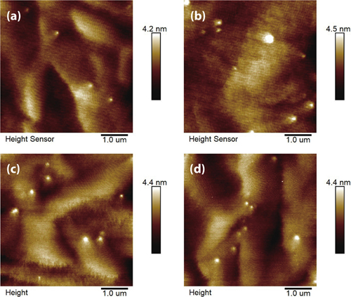
After the growth of green InGaN/GaN MQWs structures on Templates I0–I5, the surface morphologies are exhibited by AFM, as shown inFig. 4. There are some bright bumps caused by indium precipitation on the surface of all samples. Apart from that, the atomic step flow morphology can be observed in all figures, indicating that the surfaces of all four samples are smooth. The root-mean-square roughness of Sample M0, Sample M1, Sample M3 and Sample M5 is 0.609, 0.636, 0.612, and 0.671 nm, respectively. This result reveals that the introduction of nano-patterned InGaN films does not lead to degradation of the surface morphology of green InGaN/GaN MQWs structures.

Fig. 4. (Color online) The 5 × 5 µm2 AFM images of green InGaN/GaN MQWs structures of (a) Sample M0, (b) Sample M1, (c) Sample M3, and (d) Sample M5.

下载图片 查看所有图片

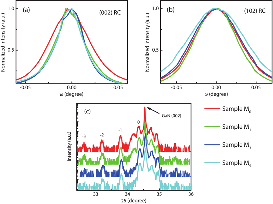
HRXRD is used to identify the crystalline quality. As we known, the full width at half maximum (FWHM) value of XRD rocking curve (RC) can characterize the dislocation density of crystal[21]. The GaN RCs of symmetric (002) and asymmetric (102) reflection for Samples M0–M5 are respectively shown inFigs. 5(a) and5(b), and the FWHM values extracted from curves as well as the accordingly calculated dislocation densities are given inTable 1. It can be seen that the nano-patterned InGaN film improves the crystalline quality of structure grown on it when the nano-pattern size is small, however, the opposite result occurs when the size becomes large. This phenomenon stems from the competition of several factors. The InGaN nano-pattern acts like the pattern of PSS during GaN growth, which can induce dislocations to bend towards the side wall, in other words, it introduces the lateral epitaxial overgrowth process to reduce dislocations propagated upward[22,23]. On the contrary, etching damage is introduced in the etching process, and dislocations are generated by GaN meeting happened at the top of the nano-pattern. It seems that the above disadvantages of nano-patterned InGaN film outweigh the advantages once the nano-pattern is of a certain size. So that the crystal qualities of Samples M3 and M5 are poor compare to Sample M0. Among them, the advantages and disadvantages almost cancel each other out in Sample M3, result in a very little bit larger dislocation density than Sample M0.Fig. 5(c) shows the (002) reflection spectra of green InGaN/GaN MQWs obtained for ω–2θ scans. The profile and distribution of the diffraction peaks can give a glance of the state of MQWs, that the intense and well-defined satellite peaks implying the abrupt and smooth interfaces between InGaN wells and GaN barriers[24]. It can be seen that Samples M0 and M1 are grown better while Sample M5 is relatively poorly. This is consistent with the results of FWHMs.

Fig. 5. (Color online) XRD results of Samples M0–M5. (a) GaN (002) reflection RC. (b) GaN (102) reflection RC. (c) Spectra of (002) ω–2θ scans.

下载图片 查看所有图片

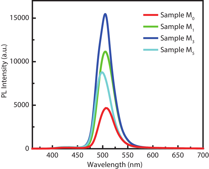
The PL spectra of green InGaN/GaN MQWs are revealed inFig. 6. Under the same test conditions, all MQWs structures grown on nano-patterned InGaN films exhibit stronger luminous than which on untreated InGaN film, and the strongest luminous intensity is about 3 times stronger than the lowest. For Sample M1, one of reasons for the enhanced luminescence may be the improvement of crystalline quality. However, this is inexplicable for Sample M3 and Sample M5 according to the aforementioned XRD results. The concave-convex InGaN film can increase the light output by introducing light scattering or refracting effect for the light generated within active region[25]. And this seems reasonable because of the fact that the crystal quality of Sample M5 has deteriorated but its luminescence is still stronger than that of the MQWs structure grown on flat InGaN layer, that is, Sample M0. Due to the small size and the dense distribution of the nano-patterns of Template I1, as shown inFig. 3(a), it has limited help to the photons in finding the escape cone. Therefore, although the crystal quality of Sample M1 is the best, its PL intensity is not the strongest. For Sample M3, the crystalline quality has not deteriorated too much, and the used Template I3 is conducive to the emission of photons, so it has the best luminous intensity. In addition, it is concerned that the uneven InGaN film may affect thermal conductivity during growth. The wavelength of Sample M5 is the shortest, which may be due to the poor heat transfer of the pattern during the low temperature growth of the InGaN well layer, resulting in poor indium incorporation. Fortunately, the nano-patterned InGaN layer has little influence on the thermal conductivity when the pattern is small, as seen in the wavelengths of Sample M1 and Sample M3.

Fig. 6. (Color online) PL spectra of Samples M0–M5 at room temperature.

下载图片 查看所有图片

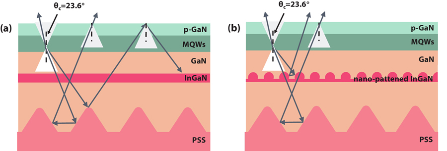
To visualize the enhancement of light output by nano-patterned InGaN, a schematic diagram of the light-emission path of green InGaN/GaN MQWs is shown inFig. 7. A portion of the light generated in MQWs cannot be emitted into the air, including light propagating downward, or light propagating upward but having an angle of incidence exceeding the critical angle and being reflected back. For sample with the untreated InGaN film, this part of the light is reflected or refracted at the interface between GaN and sapphire, changing the original propagation route, and thus has the opportunity to escape. However, there are photons that experience total internal reflection. For sample with the nano-patterned InGaN film, which acts like a second PSS, giving photons more opportunity to find the escape cone through multiple reflections or refractions. As a result, an improvement in light output can be achieved.

Fig. 7. (Color online) Schematic diagram of the light-emission path of the green InGaN/GaN MQWs (a) with untreated InGaN film and (b) with nano-patterned InGaN film.

下载图片 查看所有图片

The CL mapping images of green MQWs are processed in a unified way of color and intensity range to facilitate comparison. The information of luminous intensity and luminous uniformity of samples can be obtained from the color shading and brightness distribution. FromFig. 8, it is clear at a glance that Sample M0 has the weakest luminescence, and Sample M5 is the second weakest. In addition, the luminescence uniformity of Sample M3 is the best, and the overall brightness is slightly better than that of Sample M1. The result of CL measurement is in line with that of PL, and this also proves our theory above.

Fig. 8. (Color online) CL images of (a) Sample M0, (b) Sample M1, (c) Sample M3, and (d) Sample M5.

下载图片 查看所有图片

4 Conlusion

In this article, the flat InGaN film and the nano-patterned InGaN film etched by self-assembled Ni nano-mask were introduced in green InGaN/GaN MQWs. Three different Ni nano-masks were formed by annealing thin Ni films of different thickness (1, 3, and 5 nm). Using these self-assembled Ni nano-masks in the etching process, the different nano-patterned InGaN films were obtained. No degradation of the surface morphology was observed in the samples grown on nano-patterned InGaN. When the pattern size was small, the nano-patterned InGaN film improved the crystalline quality of sample. However, when the nano-pattern reached a certain size, the crystal quality decreased instead due to serious etching damage. It was worth mentioning that the nano-pattern benefited light output by helping photons generated within the MQWs to find the escape cones. The MQWs structure using 3 nm thick Ni film as the etching mask was found to have the best luminescence of all samples, because the fact that it balanced effects of nano-patterned InGaN film on the crystal quality and the light output. For this sample the crystal quality did not deteriorate too much, and its nano-pattern was beneficial to the photon emergent.

References

[1] NakamuraSMukaiTSenohMCandela-class high-brightness InGaN/AlGaN double-heterostructure blue-light-emitting diodesAppl Phys Lett199464168710.1063/1.111832

[2] SaitoSHashimotoRHwangJet alInGaN light-emitting diodes on c-face sapphire substrates in green gap spectral rangeAppl Phys Express2013611100410.7567/APEX.6.111004

[3] LangerTKruseAKetzerF Aet alOrigin of the “green gap”: Increasing nonradiative recombination in indium-rich GaInN/GaN quantum well structuresPhys Status Solidi C20118217010.1002/pssc.201001051

[4] KongJFengM XCaiJet alGaN grown on nano-patterned sapphire substratesJ Semicond20153604300310.1088/1674-4926/36/4/043003

[5] YamaguchiSKariyaMNittaSet alStructural properties of InN on GaN grown by metalorganic vapor-phase epitaxyJ Appl Phys199985768210.1063/1.370571

[6] HoI HStringfellowG BSolid phase immiscibility in GaInNAppl Phys Lett199669270110.1063/1.117683

[7] AlbrechtMStrunkH PWeyherJ Let alCarrier recombination at single dislocations in GaN measured by cathodoluminescence in a transmission electron microscopeJ Appl Phys200292200010.1063/1.1490618

[8] HuhCLeeK SKangE Jet alImproved light-output and electrical performance of InGaN-based light-emitting diode by microroughening of the p-GaN surfaceJ Appl Phys200393938310.1063/1.1571962

[9] NiuN HWangH BLiuJ Pet alImproved quality of InGaN/GaN multiple quantum wells by a strain relief layerJ Cryst Growth200628620910.1016/j.jcrysgro.2005.09.027

[10] WangJ XWangLZhaoWet alStudy on internal quantum efficiency of blue InGaN multiple-quantum-well with an InGaN underneath layerSci China Technol Sci20105330610.1007/s11431-010-0062-z

[11] AkasakaTGotohHKobayashiYet alInGaN quantum wells with small potential fluctuation grown on InGaN underlying layersAppl Phys Lett20068910111010.1063/1.2347115

[12] WangJ XWangLZhaoWet alUnderstanding efficiency droop effect in InGaN/GaN multiple-quantum-well blue light-emitting diodes with different degree of carrier localizationAppl Phys Lett20109720111210.1063/1.3520139

[13] LinR MLuY CYuS Fet alEnhanced extraction and efficiency of blue light-emitting diodes prepared using two-step-etched patterned sapphire substratesJ Electrochem Soc2009156H87410.1149/1.3231502

[14] KimJ YKwonM KKimJ Pet alEnhanced light extraction from triangular GaN-based light-emitting diodesIEEE Photonics Technol Lett200719186510.1109/LPT.2007.907644

[15] DuJ JXuS RPengR Set alEnhancement of optical characteristic of InGaN/GaN multiple quantum-well structures by self-growing air voidsSci China Technol Sci202164158310.1007/s11431-021-1868-7

[16] FujiiTGaoYSharmaRet alIncrease in the extraction efficiency of GaN-based light-emitting diodes via surface rougheningAppl Phys Lett20048485510.1063/1.1645992

[17] WangR JLiuDZuoZ Yet alMetal-assisted electroless fabrication of nanoporous p-GaN for increasing the light extraction efficiency of light emitting diodesAIP Adv2012201210910.1063/1.3679150

[18] TaoH CXuS RMaoWet alImproved crystal quality of nonpolar a-plane GaN based on the nano pattern formed by the annealed thin Ni layerSuperlattices Microstruct201913053910.1016/j.spmi.2019.05.020

[19] CareyJ DOngL LSilvaS PFormation of low-temperature self-organized nanoscale nickel metal IslandsNanotechnology200314122310.1088/0957-4484/14/11/011

[20] ChiuC HLoM HLuT Cet alNano-processing techniques applied in GaN-based light-emitting devices with self-assembly Ni nano-masksJ Lightwave Technol200826144510.1109/JLT.2008.922157

[21] MoramM AVickersM EX-ray diffraction of III-nitridesRep Prog Phys20097203650210.1088/0034-4885/72/3/036502

[22] AshbyC I HMitchellC CHanJet alLow-dislocation-density GaN from a single growth on a textured substrateAppl Phys Lett200077323310.1063/1.1325394

[23] HeC GZhaoWZhangKet alHigh-quality GaN epilayers achieved by facet-controlled epitaxial lateral overgrowth on sputtered AlN/PSS templatesACS Appl Mater Interfaces201794338610.1021/acsami.7b14801

[24] OhM SKwonM KParkI Ket alImprovement of green LED by growing p-GaN on In0.25GaN/GaN MQWs at low temperatureJ Cryst Growth200628910710.1016/j.jcrysgro.2005.10.129

[25] SchnitzerIYablonovitchECaneauCet al30% external quantum efficiency from surface textured, thin-film light-emitting diodesAppl Phys Lett199363217410.1063/1.110575

Ruoshi Peng, Shengrui Xu, Xiaomeng Fan, Hongchang Tao, Huake Su, Yuan Gao, Jincheng Zhang, Yue Hao. Application of nano-patterned InGaN fabricated by self-assembled Ni nano-masks in green InGaN/GaN multiple quantum wells[J]. Journal of Semiconductors, 2023, 44(4): 042801.

引用该论文: TXT   |   EndNote

相关论文

加载中...

关于本站 Cookie 的使用提示

中国光学期刊网使用基于 cookie 的技术来更好地为您提供各项服务,点击此处了解我们的隐私策略。 如您需继续使用本网站,请您授权我们使用本地 cookie 来保存部分信息。
全站搜索
您最值得信赖的光电行业旗舰网络服务平台!