Author Affiliations
Abstract
Wide Bandgap Semiconductor Technology Disciplines State Key Laboratory, School of Microelectronics, Xi'dian University, Xi'an 710071, China
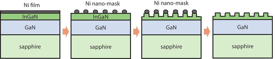
The nano-patterned InGaN film was used in green InGaN/GaN multiple quantum wells (MQWs) structure, to relieve the unpleasantly existing mismatch between high indium content InGaN and GaN, as well as to enhance the light output. The different self-assembled nano-masks were formed on InGaN by annealing thin Ni layers of different thicknesses. Whereafter, the InGaN films were etched into nano-patterned films. Compared with the green MQWs structure grown on untreated InGaN film, which on nano-patterned InGaN had better luminous performance. Among them the MQWs performed best when 3 nm thick Ni film was used as mask, because that optimally balanced the effects of nano-patterned InGaN on the crystal quality and the light output.The nano-patterned InGaN film was used in green InGaN/GaN multiple quantum wells (MQWs) structure, to relieve the unpleasantly existing mismatch between high indium content InGaN and GaN, as well as to enhance the light output. The different self-assembled nano-masks were formed on InGaN by annealing thin Ni layers of different thicknesses. Whereafter, the InGaN films were etched into nano-patterned films. Compared with the green MQWs structure grown on untreated InGaN film, which on nano-patterned InGaN had better luminous performance. Among them the MQWs performed best when 3 nm thick Ni film was used as mask, because that optimally balanced the effects of nano-patterned InGaN on the crystal quality and the light output.
GaN InGaN nano-mask nano-patterned MQWs Journal of Semiconductors
2023, 44(4): 042801
1 广东技术师范学院电子与信息学院, 广东 广州 510665
2 广东技术师范学院机电学院, 广东 广州 510665
实验中在p-GaN层制备单层密排的聚苯乙烯(PS)纳米球作为掩模,通过改变纳米球掩膜的直径,制作了周期性的占空比不同的GaN纳米圆台阵列结构。实验结果表明,在归一化激发光功率后, p-GaN层制备纳米圆台阵列的LED出光效率最高增加到参考样品的3.8倍。三维时域有限差分方法计算表明,周期性纳米结构破坏了p-GaN表面的全反射,增大了LED结构的光输出临界角,从而提高LED的光致发光效率。此外,利用可变的纳米球掩模刻蚀技术,可以在同一个周期下优化纳米圆台的尺寸从而进一步提高LED的出光效率,这可以用等效折射率与薄膜透射率理论来解释,计算结果与实验结果比较一致。
光学设计 发光二极管 纳米图形化 纳米球刻蚀 光致发光 激光与光电子学进展
2016, 53(7): 072201
北京邮电大学 信息光子学与光通信国家重点实验室, 北京 100876
采用金属有机化学气相沉积方法在无掩模的直径为400nm的圆柱Si(100)图形衬底上外延生长了GaAs薄膜。图形衬底采用纳米压印技术及反应离子刻蚀技术制作而成。运用两步法生长工艺在此图形衬底上制备了厚度为1.8μm的GaAs外延层。GaAs的晶体质量通过腐蚀坑密度和透射电镜表征。图形衬底上的 GaAs外延层表面腐蚀坑密度约1×107cm-2, 比平面衬底上降低了两个数量级。透射电镜观测显示大部分产生于GaAs/Si异质界面的穿透位错被阻挡在圆柱顶部附近。
纳米图形衬底 nano patterned substrate MOCVD MOCVD GaAs GaAs Si Si


