激光与光电子学进展, 2019, 56 (6): 060001, 网络出版: 2019-07-30
AlGaN基深紫外发光二极管空穴注入效率的提高途径  下载: 2247次封面文章
Hole Injection Efficiency Improvement for AlGaN-Based Deep Ultraviolet Light-Emitting Diodes
图 & 表
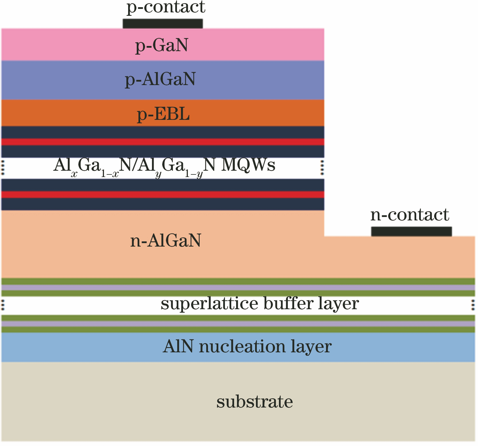
图 2. 计算结果。(a) AlxGa1-xN层的相对介电常数和不同AlN组分之间的关系;(b)平衡态时,器件A1与器件A2的隧穿结区电场强度对比图(插图是隧穿结区电场峰值强度与不同极化水平之间的关系图)。图片引自文献[ 57],已获得Wiley的版权许可
Fig. 2. Simulation results. (a) Relative dielectric constant of AlxGa1-xN layer versus AlN composition; (b) electric fields in tunneling regions for devices A1 and A2 at equilibrium (Inset shows peak field intensity versus polarization level). Reproduced from Ref. [57] with permission of Wiley

图 3. 计算结果。(a)注入电流为35 mA 时,器件A4,A5和A6隧穿结区的电场分布;(b)注入电流为35 mA时,器件A3,A4,A5和A6有源区内空穴分布;(c)器件A3,A4,A5和A6的光输出功率和注入电流之间的关系
Fig. 3. Simulation results. (a) Electric field profiles in tunneling regions for devices A4, A5, and A6 at injection current of 35 mA; (b) hole concentration profiles in active region for devices A3, A4, A5, and A6 at current injection of 35 mA; (c) light output power for devices A3, A4, A5, and A6 versus injection current

图 4. 注入电流为35 mA时,器件A3,A4,A5和A6最后一个量子阱中的横向空穴分布
Fig. 4. Lateral hole concentration profiles in last quantum well for devices A3, A4, A5, and A6 at injection current of 35 mA

图 5. 器件A3,A4,A5和A6的电流和电压特性曲线
Fig. 5. Current versus applied voltage for devices A3, A4, A5, and A6

图 6. p-AlxGa1-xN层界面耗尽区能带图和电场示意图。(a)能带图;(b)电场示意图。图片引自文献[ 58],已获得Optical Society of America的版权许可
Fig. 6. Energy band diagram and electric field profile in interface depletion region of p-AlxGa1-xN layer. (a) Energy band diagram; (b) schematic of electric field profile. Reproduced from Ref. [58] with permission of Optical Society of America

图 7. 计算结果。(a) 5组DUV LED器件结构的空穴供给层中对应的电场分布;(b)注入电流为200 A·cm-2时,5组DUV LED器件理论计算得到的光功率。图片7(a)引自文献[ 58],已获得Optical Society of America的版权许可。图片7(b)引自文献[ 4],具体数值总结于文献[ 58]
Fig. 7. Simulation results. (a) Electric field profiles in hole supplier layer for five groups of DUV LED devices; (b) calculated power densities for five groups of DUV LED devices at injection current of 200 A·cm-2. (a) is reproduced from Ref. [58] with permission of Optical Society of America. (b) is reproduced from Ref. [4], and the value is summarized according to the report in Ref. [58]

图 8. I-V特性对比图。(a) Original device和Reference device;(b) Reference Device和器件B1;(c) Reference Device,器件B2和B3。图片引自文献[ 58],已获得Optical Society of America的版权许可
Fig. 8. I-V characteristic comparison. (a) Original device and Reference device; (b) Reference device and device B1; (c) Reference device, device B2 and device B3. Reproduced from Ref. [58] with permission of Optical Society of America

图 9. 示意图和计算结果。(a)传统的p-EBL和(b)具有p-AlxGa1-xN/AlyGa1-yN/AlxGa1-xN(x>y)EBL的DUV LED器件的能带示意图;(c) p-EBL和p-AlGaN层的空穴分布图。图片引自文献[ 59],已获得 American Chemical Society的版权许可
Fig. 9. Schematic and simulation results. Schematic of energy bands for (a) DUV LED with the conventional p-EBL and (b) DUV LED with the p-AlxGa1-xN/AlyGa1-yN/AlxGa1-xN (x>y) EBL; (c) hole concentration profiles in p-EBL and p-AlGaN layers. Reproduced from Ref. [59] with permission of American Chemical Society

图 10. 计算结果和实验结果。(a)器件C1和器件C2量子阱中空穴浓度分布图;(b)实验测得的器件C1和器件C2的光输出功率和EQE;(c)理论计算得到的器件C1和器件C2的光输出功率和EQE。图片引自文献[ 59],已获得American Chemical Society的版权许可
Fig. 10. Simulation and experimental results. (a) Hole concentration profiles in quantum wells for devices C1 and C2; (b) measured optical power and EQE for devices C1 and C2; (c) calculated optical power and EQE for devices C1 and C2. Reproduced from Ref. [59] with permission of American Chemical Society

图 11. 注入电流为 35mA时计算结果。(a) DUV LED器件光输出功率与极化水平之间的关系;(b)器件D1,D2,D3,D4和D5的量子阱,及p-AlGaN层和p-GaN层中空穴分布图。图片引自文献[ 79],已获得Elsevier的版权许可
Fig. 11. Simulation results at injection current of 35 mA. (a) Light output power for DUV LEDs in terms of the polarization level; (b) hole concentration profiles in quantum wells, p-AlGaN layer and p-GaN layer for devices D1, D2, D3, D4, and D5. Reproduced from Ref. [79] with permission of Elsevier

图 12. 注入电流为35 mA时的计算结果。(a) DUV LED器件光输出功率和p-EBL/p-AlGaN/p-GaN界面处的极化水平之间的关系;(b)器件 D6,D7,D8和 D9量子阱和p-AlGaN/p-GaN层中空穴分布;(c)器件 D6,D7,D8和 D9的电场分布图。图片引自文献[ 79],已获得Elsevier的版权许可
Fig. 12. Simulation results at injection current of 35 mA. (a) Light output power for DUV LED versus polarization level at p-EBL/p-AlGaN/p-GaN interface; (b) hole concentration profiles in quantum well, p-AlGaN layer and p-GaN layer for devices D6, D7, D8, and D9; (c) electric field profiles for devices D6, D7, D8, and D9. Reproduced from Ref. [79] with permission of Elsevier

图 13. 注入电流密度为100 A/cm2时,器件E1,E2和E3量子阱中的载流子分布。(a)电子分布;(b)空穴分布。图片引自文献[ 83],已获得Optical Society of America的版权许可
Fig. 13. Carrier concentration profiles for devices E1, E2, and E3 at injection current of 100 A/cm2. (a) Electron profiles; (b) hole profiles. Reproduced from Ref. [83] with permission of Optical Society of America

图 14. 能带示意图与光输出功率。(a) UVA LED器件能带示意图;(b)器件E1,E2和E3实验(曲线)和理论(散点)计算得到的光输出功率。图片引自文献[ 84],已获得Optical Society of America的版权许可
Fig. 14. Energy band diagram and optical output power. (a) Schematic of energy bands for UVA LED; (b) measured (curve) and calculated (scatterplot) optical powers for devices E1,E2, and E3 in terms of current. Reproduced from Ref. [84] with permission of Optical Society of America

表 1具有不同AlN组分的p-EBL和p-AlxGa1-xN层的器件结构。表格引自文献[ 58],已获得Optical Society of America的版权许可
Table1. Devices with different AlN compositions for p-EBL and the p-AlxGa1-xN layers. Reproduced from Ref. [58] with permission of Optical Society of America
|
表 2注入电流为35 mA时,器件D6,D7,D8和D9的p-AlGaN/p-GaN层中的电场对空穴的做功。表格引自文献[ 79],已获得Elsevier的版权许可
Table2. Work done to holes by electric field within p-AlGaN/p-GaN structure for devices D6, D7, D8, and D9 at injection current of 35 mA. Reproduced from Ref. [79] with permission of Elsevier
|
田康凯, 楚春双, 毕文刚, 张勇辉, 张紫辉. AlGaN基深紫外发光二极管空穴注入效率的提高途径[J]. 激光与光电子学进展, 2019, 56(6): 060001. Kangkai Tian, Chunshuang Chu, Wengang Bi, Yonghui Zhang, Zihui Zhang. Hole Injection Efficiency Improvement for AlGaN-Based Deep Ultraviolet Light-Emitting Diodes[J]. Laser & Optoelectronics Progress, 2019, 56(6): 060001.


 PDF全文
PDF全文

