Author Affiliations
Abstract
1 School of Microelectronics, University of Science and Technology of China, Hefei 230026, China
2 Dynax Semiconductor Inc., Suzhou 215300, China
3 Department of Micro- and Nanoelectronics, Saint Petersburg Electrotechnical University, Saint Petersburg 197376, Russia
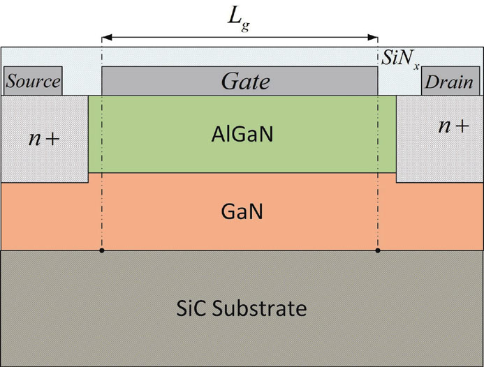
A physics-based analytical expression that predicts the charge, electrical field and potential distributions along the gated region of the GaN HEMT channel has been developed. Unlike the gradual channel approximation (GCA), the proposed model considers the non-uniform variation of the concentration under the gated region as a function of terminal applied voltages. In addition, the model can capture the influence of mobility and channel temperature on the charge distribution trend. The comparison with the hydrodynamic (HD) numerical simulation showed a high agreement of the proposed model with numerical data for different bias conditions considering the self-heating and quantization of the electron concentration. The analytical nature of the model allows us to reduce the computational and time cost of the simulation. Also, it can be used as a core expression to develop a complete physics-based transistor Ⅳ model without GCA limitation.
AlGaN/GaN (HEMTs) 2DEG charge distribution electron mobility hydrodynamic model channel temperature Journal of Semiconductors
2023, 44(8): 082802
红外与毫米波学报
2022, 41(6): 1037

Author Affiliations
Abstract
MOE Key Laboratory of Weak-Light Nonlinear Photonics, TEDA Institute of Applied Physics and School of Physics, Nankai University, Tianjin 300457, China
Holographic display has attracted widespread interest because of its ability to show the complete information of the object and bring people an unprecedented sense of presence. The absence of ideal recording materials has hampered the realization of their commercial applications. Here we report that the response time of a bismuth and magnesium co-doped lithium niobate (LN:Bi,Mg) crystal is shortened to 7.2 ms and a sensitivity as high as 646 cm/J. The crystal was used to demonstrate a real-time holographic display with a refresh rate of 60 Hz, as that of the popular high-definition television. Moreover, the first-principles calculations indicate that the electron mobility while Bi occupying Nb-site is significantly greater than that in Li-site, which directly induces the fast response of LN:Bi,Mg crystals when the concentration of Mg is above its doping threshold.Holographic display has attracted widespread interest because of its ability to show the complete information of the object and bring people an unprecedented sense of presence. The absence of ideal recording materials has hampered the realization of their commercial applications. Here we report that the response time of a bismuth and magnesium co-doped lithium niobate (LN:Bi,Mg) crystal is shortened to 7.2 ms and a sensitivity as high as 646 cm/J. The crystal was used to demonstrate a real-time holographic display with a refresh rate of 60 Hz, as that of the popular high-definition television. Moreover, the first-principles calculations indicate that the electron mobility while Bi occupying Nb-site is significantly greater than that in Li-site, which directly induces the fast response of LN:Bi,Mg crystals when the concentration of Mg is above its doping threshold.
holographic display lithium niobate photorefractive electron mobility Opto-Electronic Advances
2022, 5(12): 210135
1 中国科学院上海微系统与信息技术研究所 中科院太赫兹固态技术重点实验室,上海 200050
2 中国科学院大学 材料科学与光电子工程中心,北京 100049
3 海南师范大学 材料科学与光电工程研究中心,海南 海口 571158
采用气体源分子束外延(GSMBE)技术,研究了InP衬底上InyAl1-yAs线性渐变缓冲层对In0.66Ga0.34As/InyAl1-yAs高迁移率晶体管(HEMT)材料特性影响。研究了不同厚度和不同铟含量的InyAl1-yAs线性渐变缓冲层对材料的表面质量、电子迁移率和二维电子气浓度的影响。结果表明,在300 K(77 K)时,电子迁移率和电子浓度分别为8 570 cm2/(Vs)-1(23 200 cm2/(Vs)-1)3.255E12 cm-2(2.732E12 cm-2)。当InyAl1-yAs线性渐变缓冲层厚度为50 nm时,材料的表面形貌得到了很好的改善,均方根粗糙度(RMS)为0.154 nm。本研究可以为HEMT器件性能的提高提供强有力的支持。
InyAl1-yAs线性渐变缓冲层 磷化铟 高电子迁移率场效应晶体管 InyAl1-yAs graded buffer layer InP high electron mobility transistor(HEMT)
1 西安电子科技大学 a.机电工程学院
2 b.宽禁带半导体技术国家重点实验室, 陕西西安 710071
3 西安电子科技大学 b.宽禁带半导体技术国家重点实验室, 陕西西安 710071
GaN基高电子迁移率晶体管(HEMT)器件具有抗高频、耐高温、大功率、抗辐射等特性, 在核反应堆、宇宙探测等辐射环境中具有广阔的应用前景。借助 SRIM软件仿真 1.8 MeV质子辐射对不同 AlGaN势垒层纵向尺寸下的常规耗尽型器件内部产生空位密度的影响, 并观察空位密度随深度的变化规律。在最优 AlGaN势垒层厚度条件下, 通过仿真对比 5种不同栅氧层材料的 MIS-HEMT器件, 发现氮化铝(AlN)栅氧层材料具有相对较好的抗辐射效果。
GaN材料 HEMT器件 MIS-HEMT器件 质子辐射仿真 material of GaN High Electron Mobility Transistor Metal Insulator Semiconductor -HEMT proton radiation simulation 太赫兹科学与电子信息学报
2022, 20(9): 922


