硅异质结太阳能电池工艺优化  下载: 565次
0 Introduction
Advantages of Silicon Heterojunction (SHJ) solar cells are its symmetrical structure and low temperature process, a very high energy conversion efficiency potential (>25%)[1-4], a low temperature coefficient and a good stability under light and thermal exposure. Optical and electrical enhancements are two typical ways to enhance the conversion efficiency of the solar cells. Over the past few years, many researchers joined this field, which accelerated and deepened the fundamental knowledge about this structure[5-7]. SHJ solar cell technology involves many processes, from wafer wet-chemical treatment, passivation to electrode fabrication. The recombination loss affect significantly solar cell performances, more particularly the Fill Factor (FF), but also the open-circuit voltage (VOC). Intrinsic hydrogenated amorphous silicon layer i-a-Si:H passivation quality have an impact on the interface recombination and thus affect the open circuit voltage (VOC) of the final solar cell[8-10]. As the window layer of the SHJ solar cells, the p-type amorphous film also requires a wide band gap to reduce the parasitic absorption and improve the short wavelength photo-response of the solar cells. Low carrier concentration and high carrier mobility of Indium Tin Oxides (ITO) (Sn:In2O3) film are also necessary for reducing the free carrier absorption, thereby increasing photo-response in the longer wavelength range[11]. So far, there are few systematic studies on SHJ solar cells by step-by-step analysis.
Here, starting from the saw damage and pyramid etched Si wafer to the complete device, we optimize the performance of SHJ solar cells by step-by-step analysis. Optimum pyramid size for passivation of surface was obtained. Silicon wafer was passivated with high quality amorphous silicon layer. To reduce the parasitic absorption and improve the short wavelength response of the solar cells, large band gap p-type a-SiCx:H was applied as emitter layer alternative to p-type a-Si:H film. By regulating ITO Physical Vapor Deposition (PVD) process, low carrier concentration and high carrier mobility was obtained. We optimized the carrier concentration of ITO, as low as half value of ordinary ITO, obviously reducing the free carrier absorption and boost the External Quantum Efficiency (EQE) in the longer wavelength range. Based on these optimizations, SHJ solar cells with a high conversion efficiency were prepared.
1 Experimental
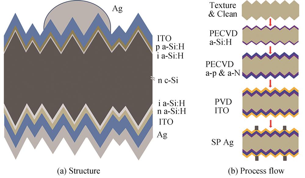
As-cut c-Si wafer (Czochralski grown, mono-crystalline, n-type, Si(100), diameter 5 inch (1 inch=2.54 cm), initial thickness 130~150 μm, resistivity 1~5 Ω·cm) was handled by wet-chemical processes, including removal of saw damage and a random pyramid surface texture etching. For the removal of saw damages, the as-cut samples were etched in aqueous solution of KOH (wt. 20%) at 75℃ for 10 s. Subsequently, random pyramid textured substrate surfaces were prepared in a lower concentration of KOH solution at 80℃ with TS45 as an additive. Afterward, the wafers were cleaned according to the modified Radio Corporation of American (RCA) process. Owing to its property of being easily oxidized, the prepared c-Si wafer was dipped in diluted hydrofluoric acid (5%, 1 min) immediately. Hydrogenated amorphous silicon (a-Si:H) layers were deposited by the standard Plasma Enhanced Chemical Vapor Deposition (PECVD) process at different temperatures (180, 200, 220 and 240℃). The n-type and p-type a-Si:H films were deposited by doping PH3 or B2H6 diluted with H2 and SiH4, respectively. Thus, heterojunctions with emitter layer, intrinsic layers and a-Si:H Back Surface Field (BSF) of the sequence (n) a-Si:H/(i) a-Si:H/(n) c-Si/(i) a-Si:H/(p)a-Si:H were formed.
For the solar cell preparation of Transparent Conductive Oxides (TCO) layers, ITO film (100 nm) were prepared by DC magnetron sputter deposition on both side of wafer with addition of < 1.0% oxygen to the Ar sputter gas without additional sample heating[11]. The rear contact was prepared by evaporating a 500 nm Ag film. The preparation of 1 cm×1 cm solar cells was completed by evaporated 1 μm Ag front grid lines.
A Field Emission Scanning Electron Microscopy (FESEM, HITACHI, SU-8020) was used to investigate morphological of the textured solar cell substrates. The thickness of the film has been measured by using Veeco Profiler (Dektak 150). WCT-120 lifetime tester from Sinton Instruments was applied for minority carrier lifetime test. The photovoltaic performance was characterized under a simulated sunlight illumination generated by a SAN-EI ELECTRIC XES-40S2-CE Solar Simulator (AM 1.5 G filter at 100 mW/cm2), which was calibrated using a certified silicon photodiode before used. J-V characteristics were obtained by using Keithley 2 400 source meter.
2 Results and discussion
2.1 Structure and process flow of SHJ solar cell
2.2 Wet-chemical treatment
Wet-chemical processes include removal of saw damage and a random pyramid surface texture etching. Sawing of the monocrystalline Si ingot into wafers contaminates the surfaces with the cutting slurry and creates crystal damages at the surfaces, as seen in
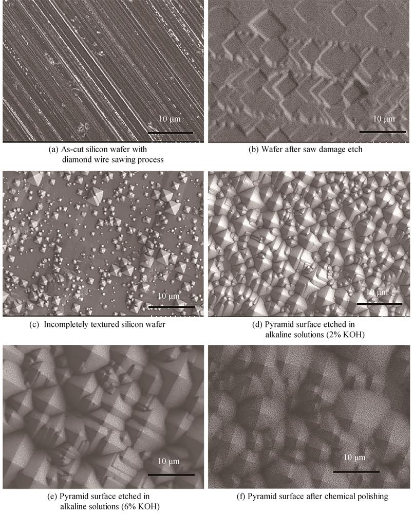
图 2.
Fig. 2. SEM image of as-cut silicon wafer, wafer after saw damage etch, incompletely textured wafer, pyramid surface etched in 2% and 6% alkaline solutions and after chemical polishing
To improve the light trapping and thereby enhance the short-circuit current densities of the SHJ solar cell, particular emphasis is put on the wet-chemical random pyramid texturization of the solar cell substrates. Moreover, defects and contaminations on the surface can already be drastically reduced during the texturing process. Surface texturing is conventionally achieved by anisotropic wet-chemical etching of Si(100) wafers in alkaline solutions containing Isopropyl Alcohol (IPA) as an additive. Pyramid formation is due to the anisotropic reaction of alkali and silicon. In a certain concentration of alkaline solution, the reaction speed of OH- with the (100) surface of silicon is faster than that of the (111) surface. That is why the pyramid structure is formed[13].
2.3 Interface passivation
Key feature of SHJ solar cell concept is a thin intrinsic amorphous hydrogenated silicon ((i) a-Si:H) layer which forms the heterocontact with a crystalline silicon (c-Si) wafer, provides passivation of the a-Si:H/c-Si interface, thus enables high open-circuit voltages (Voc). Further optimization of the a-Si:H/c-Si interface lead to an increase of the Voc, thereby an improvement of the solar cell performance[14]. A common technique to characterize the interface quality is to measure the carrier lifetime τeff as a function of the minority excess charge carrier density Δn by means of Transient Photoconductance Decay (TrPCD)[15].
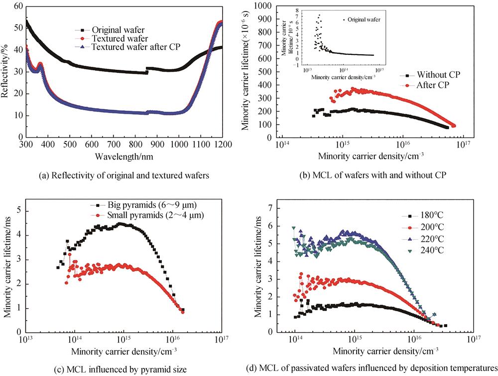
图 3.
Fig. 3. Reflectivity of original and textured wafers, MCL of passivated wafers affected by chemical polishing, pyramidsize and a-Si:H deposited at different temperatures
Optimization of texturization and cleaning was followed by intrinsic a-Si:H layers deposition, which are known to provide excellent passivation of the c-Si surfaces, causing a decrease of interface state density, mainly by hydrogenation of silicon dangling bonds. The a-Si:H thin film samples were prepared in a Radio Frequency (RF) 13.56 MHz and power density of 0.16 W/cm2 capacitive-coupled PECVD system. We deposited the textured wafer with the percentage content of silane SiH4 and dydrogen H2 at 220℃ under the chamber pressure of 1.5 (1 Torr=133.322 Pa). To get a high quality of a-Si:H passivated wafer, the window of deposition process is rather narrow. The influence of pyramid size on the effective minority charge carrier lifetime τeff after passivating with a-Si:H layer is summarized in
The influence of the deposition temperature on τeff of textured c-Si wafers is shown in
2.4 Emitter and ITO optimization
In order to improve short wavelength photoresponse, p-type a-SiCx:H emitter was used in the SHJ solar cell absorption alternative to p-type a-Si:H[20]. Due to its broad band gap, the EQE of SHJ solar cell with p-type a-SiCx:H as emitter layer in short wavelength range of 300 to 600 nm is significantly higher than using p-type a-Si:H, as seen in
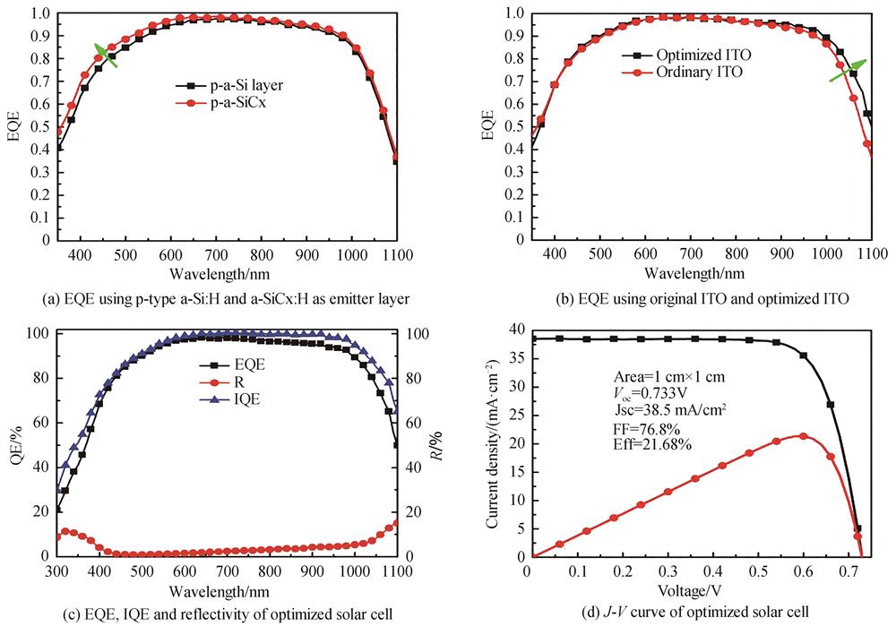
Eventually ITO layers were deposited on top Nip and back niN of the layer stack, respectively. ITO parasitic absorption in SHJ solar cell mainly includes the belt edge absorption and free carrier absorption. The former mainly affects the absorption of SHJ in the short wave region, while the latter affects the absorption in the long wave region. By 200℃ annealing after both the rear and front side ITO deposition, the ITO layer doping concentration was optimized to obtain a trade-off between low parasitic free-carrier absorption and low resistivity. The resistivity of 2.5×10⁻⁴ Ω·cm, highest carrier mobility of 31.8 cm2·V-1·s-1 and carrier concentration of 6.9×1020 cm-3 were obtained at Ar(O2) gas flow rate of 20 Sccm with the working pressure of 0.002 Torr. Using the optimized ITO layer with high charge carrier mobility and low resistivity in SHJ solar cell, the long wavelength response was obviously enhanced due to decrease of free carrier absorption, as shown in
After metallic contacts were prepared and the characteristics of the solar cell were determined, the J-V curves of the 1 cm×1 cm cells were measured under standard test conditions with a shadow mask. The results of the best solar cell are given in
4 Conclusion
Step-by-step optimization were analysed throughout the processing of SHJ solar cells starting from the pyramid structure etched Si wafer to the complete solar cell. Based on this investigation, recombination losses were successfully minimized and high open-circuit voltages and fill factors were obtained. Power conversion efficiencies above 21.68% were achieved by optimization of the texturing of silicon wafers, interface passivation, broad band gap emitter and ITO adjusting. The use of the silk-screen printing would be beneficial for further improvement of the solar cell.
[14] DING Yueke, HUANG Shihua. Study on passivation of monocrystalline silicon by tandem hydrogenated amorphous silicon film[J]. Acta Photonica Sinica, 2021, 50(3): 0331001.
Article Outline
张喜生, 晏春愉, 王景州, 马紫微, 姚陈忠. 硅异质结太阳能电池工艺优化[J]. 光子学报, 2021, 50(12): 1223001. Xisheng ZHANG, Chunyu YAN, Jingzhou WANG, Ziwei MA, Chenzhong YAO. Optimizing Processes of Silicon Heterojunction Solar Cell[J]. ACTA PHOTONICA SINICA, 2021, 50(12): 1223001.


 PDF全文
PDF全文
