杂化泛函HSE和PBE0计算CsPbI3缺陷性质的比较研究
Over the past decade, halide perovskite materials, represented by CH3NH3PbI3, have made significant progress in the field of new solar cell materials. These materials do not contain any rare elements, and can be fabricated by low-cost methods[1⇓⇓⇓⇓-6]. In 2009, Miyasaka group[7] achieved a photoelectric conversion efficiency of 3.8%. In 2013, Grätzel and Snaith group[2,8] achieved an efficiency of 15% using different cell structures. Recently, the highest efficiency of perovskite solar cells verified by the US National Renewable Energy Laboratory has reached 25.7%, which is close to the record of silicon-based cells (26.7%)[9]. Currently, halide perovskite solar cells still face some urgent problems, including material stability, lead toxicity, and efficiency reduction in large-scale cells. Despite These problems, the ability of halide perovskite solar cells to achieve such high efficiency in a short period of time is still unprecedented in the history of solar cell development.
The halide perovskite materials also exhibit promising properties as luminescent materials. Research on the luminescence properties of these materials dates back to 1977[10]. In 1994, the first organic-inorganic hybrid layered halide perovskite-based light-emitting diode (LED) was reported[11]. In 2014, with the significant progress in perovskite photovoltaics, an infrared LED based on CH3NH3PbI3 was achieved at room temperature[12]. In 2018, quantum efficiencies higher than 20% were achieved in perovskite infrared and green LEDs through submicron structural design and compositional engineering[13-14]. Moreover, halide perovskite materials have also received widespread attentions in fields such as light detection and high-energy particle detection[15⇓-17].
It is worthwhile noting that these materials with excellent properties can be prepared by a relatively inexpensive solution method. Such synthesis method may introduce a substantial number of defects into halide perovskites. The development of traditional semiconductor materials is often limited by the control on defects, whereas halide perovskite materials exhibit high degree of tolerance to defects[18⇓⇓⇓⇓⇓⇓-25]. Theoretical calculations based on first-principles also support this view. For example, computational studies of CH3NH3PbI3 have found that the intrinsic defects tend to form shallow energy levels, which do not significantly contribute to carrier recombination. Deep energy levels in these materials are typically associated with Pb dimers or I trimers, which tend to occur only when the Fermi level is close to the band edges[26-27]. Therefore, in halide perovskite materials, which are commonly insulators (i.e., having the Fermi level near the center of the bandgap), defects with deep energy level may not appear.
First-principles calculations based on density functional theory (DFT) are the main method to study the properties of point defects in semiconductor materials. Hybrid functionals have become a frequently used method in the study of point defects in semiconductor materials due to their accurate treatment of band gap. Combined with the spin-orbit coupling (SOC) effect, hybrid functionals can obtain band gaps that agree with experimental measurements[25]. However, to obtain band gaps that are consistent with experiments, parameters controlling the Hartree-Fock exchange energy ratio (denoted as α) need to be adjusted. Typically, α is set to 0.43 for the screened hybrid functional HSE calculations, and α is set to around 0.2 for the unscreened hybrid functional PBE0 calculations[28⇓⇓⇓⇓⇓⇓⇓-36]. The results obtained from these two methods have been discussed in bulk property calculations[37]. Their difference in defect calculations has also been reported for the organic-inorganic hybrid perovskite materials[38]. However, due to the uncertainty of structures of the organic cations at 0 K, the mechanism behind this difference remains unclear.
In recent years, pure inorganic halide perovskite materials that do not contain organic cations (such as CH3NH3+ and NH2CHNH2+) have rapidly developed[39⇓⇓⇓⇓⇓⇓-46]. They not only possess higher thermodynamic stability but also avoid the potential volatility of organic cations[47-48]. Among pure inorganic halide perovskite materials, CsPbI3 has a suitable band gap for the preparation of solar cells, and the efficiency of this material has exceeded 21%[49]. In this study, the defect transition levels (DTL) of all point defects for CsPbI3 calculated by HSE-0.43 and PBE0-0.2 functionals were compared to determine the effective method to accurately calculate the defect properties of halide perovskite.
1 Computation method
The VASP package was used in this work[50] and the orthorhombic phase of CsPbI3 (i.e., γ-CsPbI3) was considered. The interaction between ions and valence electrons was described by PAW potentials[51-52]. In calculations a plane-wave basis set was used, and changes in the volume or shape of the cell were considered. The plane-wave cutoff energy was set to 408 eV (approximately 30 Ry) for calculations with varying cell parameters, and 238 eV for calculations with fixed cell parameters. The screened hybrid functional HSE and the unscreened hybrid functional PBE0 were compared. As mentioned above, the Hartree-Fock exchange energy mixing parameter α was set to 0.43 (denoted as HSE-0.43) in the HSE calculation, while it was set to 0.2 (denoted as PBE0-0.2) in the PBE0 calculation. Except for the cell parameter optimization, all calculations included the SOC effect.
The equilibrium volume of the primitive cell was obtained by fitting the Murnaghan equation of state. The fitting used nine data points distributed uniformly within ±12% of the equilibrium volume. For structural optimization of each data point, the lattice constants are allowed to vary while the cell volume was fixed. The bulk modulus of the material can also be obtained from the fitting of the equation of state. After obtaining the equilibrium volume through fitting, the parameters of the primitive cell and internal structural parameters were further optimized. The convergence criteria for total energy and forces were set to 1.36×10⁻⁷ eV and 5.14×10⁻² eV/nm (approximately 2×10⁻⁴ Ry/Bohr), respectively. The Brillouin zone was sampled using a 3×2×3 k-grid centered at the Γ point.
The band structure calculations were performed using the 3×2×3 k-grid amended with the k-points on the high-symmetry paths, whose weights were set to zero. The effective masses were obtained by parabolic fitting of the bands near the Γ point using six data points (including Γ). The density of states and dielectric constant were calculated using a 5×4×5 k-grid and 720 bands which contain 544 valence bands. It was found that the choices of k-grid (3×2×3 or 5×4×5) and plane wave cutoff energies (408 or 238 eV) have insignificant effects on the band gap width (<0.01 eV).
Defect calculations were performed using the supercell method. A supercell containing 160 atoms was constructed from a primitive cell of 20 atoms using a transformation matrix (2 0 0 | 0 1 -1 | 0 2 2). The Brillouin zone of the supercell was represented by the Γ point. Structural relaxations were carried out using hybrid functionals combined with the SOC effect until the forces on all atoms were less than 0.257 eV/nm. To perform batch calculations using hybrid functional combined with the SOC effect, the PREC and PRECFOCK parameters were set to Normal and Fast, respectively. The DTL calculation was performed using the formula
where $E_{\text{D}}^{q}$ and $E_{\text{D}}^{{{q}'}}$ represent the total energy of point defects with charge state q and ${q}'$, respectively, and EVBM is the Kohn-Sham eigenvalue at the valence band maximum of defect-free γ-CsPbI3. Further details on the defect calculation method can be found in references[27,53].
2 Results and discussion
Fig. 1 shows the E-V relationship between the unit cell volume and total energy. The data points are obtained from hybrid functional calculations without the SOC effects, and the curve represents the result fitted by the Murnaghan equation of state. It can be seen that the curves obtained by two functionals, HSE-0.43 and PBE0-0.2, are similar, and the fitted bulk modulus (B0) values are 14.1 and 13.3 GPa, respectively, indicating that CsPbI3 is a soft material.
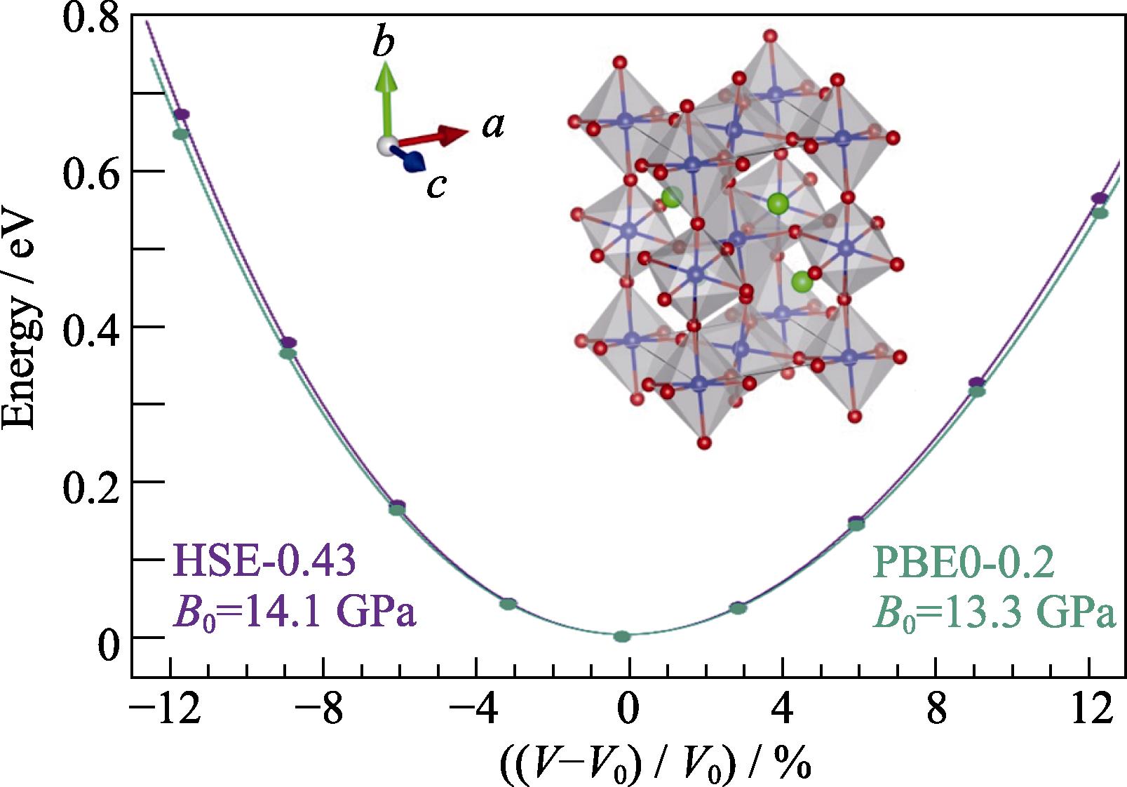
图 1.
Fig. 1. Fitting Murnaghan equation of state to obtain the equilibrium volume and bulk modulus with inset showing the atomic structure of γ -phase CsPbI3
Based on the equilibrium volume obtained by fitting the Murnaghan equation of state, primitive cell optimization was performed, and it was found that the lattice constants obtained by PBE0-0.2 are slightly larger than those obtained by HSE-0.43, as shown in Table 1. The differences in internal structural parameters obtained by two methods are less than 0.2%.
表 1.
Lattice constants and internal parameters of orthorhombic CsPbI3 calculated by two different hybrid functionals
Table 1.
Lattice constants and internal parameters of orthorhombic CsPbI3 calculated by two different hybrid functionals
| ||||||||||||||||||||||||||||||||||||||||||||||||
Fig. 2 compares the band structures obtained by two methods. Since the calculations combining hybrid functionals and SOC require high computational cost, only energy bands along the three main axes from the Γ point were considered. The direct band gap at the Γ point obtained by HSE-0.43 and PBE0-0.2 are 1.71 and 1.68 eV, respectively. The band structures obtained by two methods are similar, with the main difference being that the valence band width obtained by HSE-0.43 (about 4.2 eV) is broader than that obtained by PBE0-0.2 (about 3.8 eV).
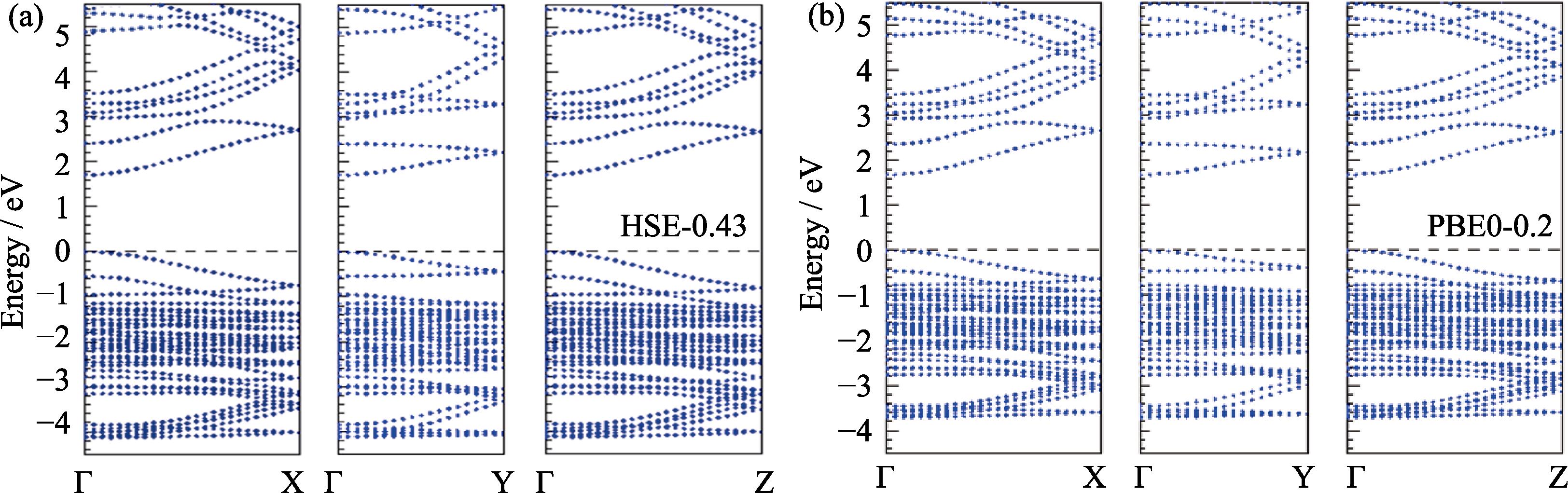
图 2.
Fig. 2. Band structures of γ -CsPbI3 calculated by two hybrid functionals HSE-0.43 (a) and PBE0-0.2 (b) including the SOC effect
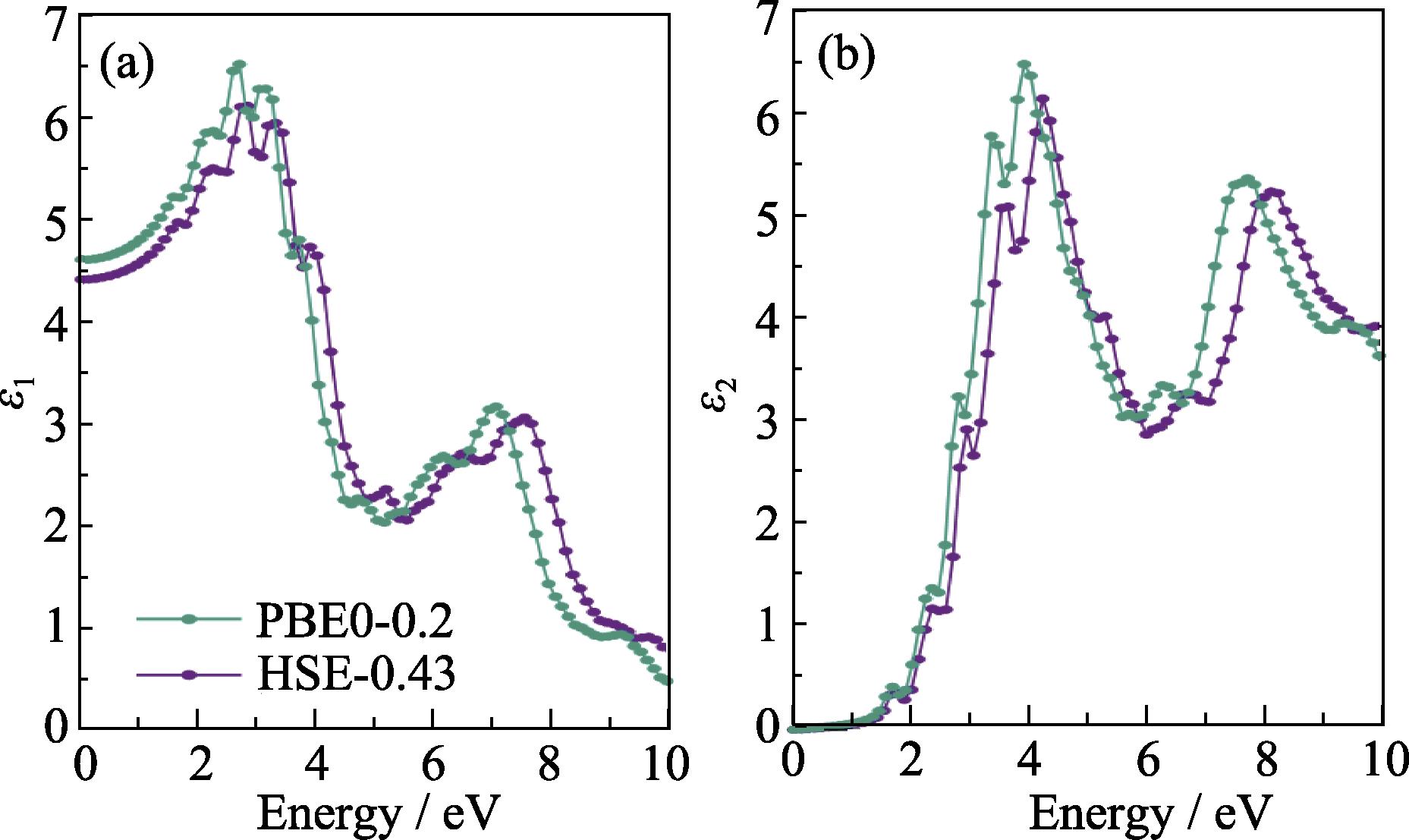
Fig. S1 in the supporting materials compares the density of states (DOS) obtained by two methods. Except for the smaller valence band width obtained by PBE0-0.2, there are no other significant differences. Fig. S2 compares the effective masses calculated by two methods. The electron effective masses obtained by HSE-0.43 are (0.17-0.19)m0, while the hole effective masses are (0.20-0.23)m0. The corresponding values obtained by PBE0-0.2 differ from the HSE-0.43 results by less than 0.1m0. Fig. S3 shows the real (ε1) and imaginary (ε2) parts of the dielectric constant. There is a slight difference in the bulk dielectric constant calculated by the HSE-0.43 and PBE0-0.2 functionals. At 0 eV, ε1 is 4.4 and 4.6 from HSE-0.43 and PBE0-0.2, respectively. The slight shift of ε2 obtained by the two methods is related to the slight difference in the band gaps.
Next, the differences between two methods in defect property calculations are discussed. In this study, vacancies of Cs, Pb, and I atoms (vCs, vPb, and vI), interstitial atoms (Csi, Pbi, and Ii), and anti-site defects (CsPb, PbCs, CsI, ICs, PbI, and IPb) are considered. As shown in Table 1, there are two symmetric positions for I atoms in the orthorhombic phase CsPbI3, denoted as I1 and I2. Both positions were considered for defect calculations, and the one with lower energy were chosen to show the results.
We focus on shallow-level defects in this work. For deep-level defects, their positions in the band gap are affected by the interaction between periodic image charges, which is not the topic of discussion in this work. Previous studies have found that deep-level defects in CsPbI3 are often accompanied by the formation of Pb dimers and I trimers[26-27]. Therefore, the defect structures without the above-mentioned structural distortions were discussed, even if the structure is metastable. Fig. 3 shows the structures of intrinsic defects in neutral charge state, where no Pb dimers and I trimers appear. Since the defect structures obtained by two methods are similar, only the structures after relaxation with PBE-0.2 are shown in Fig. 3.
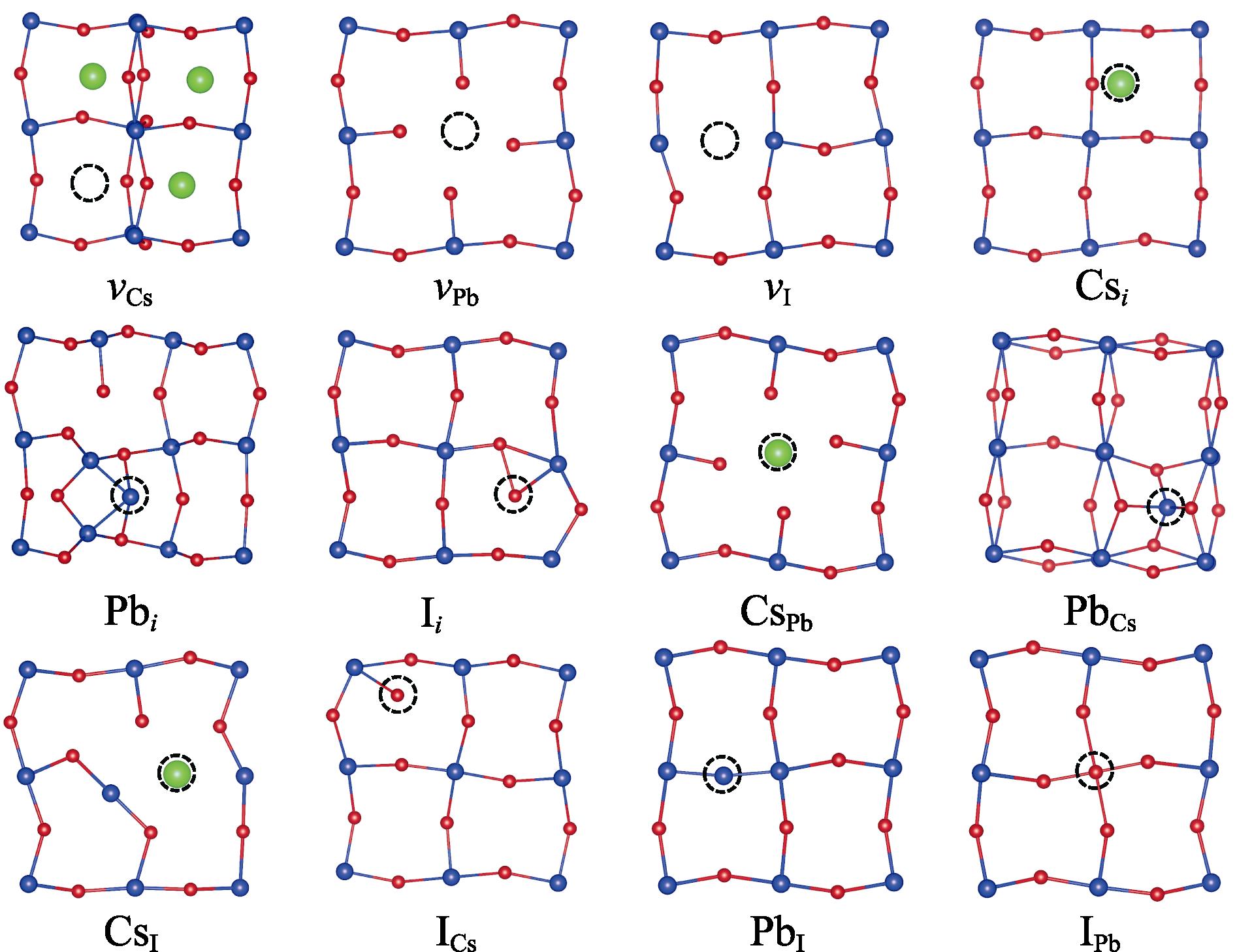
图 3.
Fig. 3. Atomic structures of 12 intrinsic defects after relaxation in neutral charge stateAs two functionals yield similar structures, only the structures from PBE0-0.2 calculations are shown here
Fig. 4(a) shows the DTLs obtained by the HSE-0.43 functional for each defect. We only consider the transition from −1 to 0, ε(−/0), for the acceptors and from 0 to +1, ε(0/+), for the donors, as these two transition levels are most directly related to the nonradiative recombination of charge carriers[53]. As can be seen, in the absence of Pb dimers and I trimers, DTLs calculated by HSE-0.43 are all shallow-level defects, except for the slightly deep ε(−/0) level of Ii. Fig. 4(b) shows DTLs calculated by the PBE0-0.2 hybrid functional, which exhibit a clear contrast with the results of HSE-0.43. Firstly, ε(−/0) levels of all acceptor defects are significantly deeper, and ε(0/+) levels of all donor defects except for Pbi and PbI are also deeper.
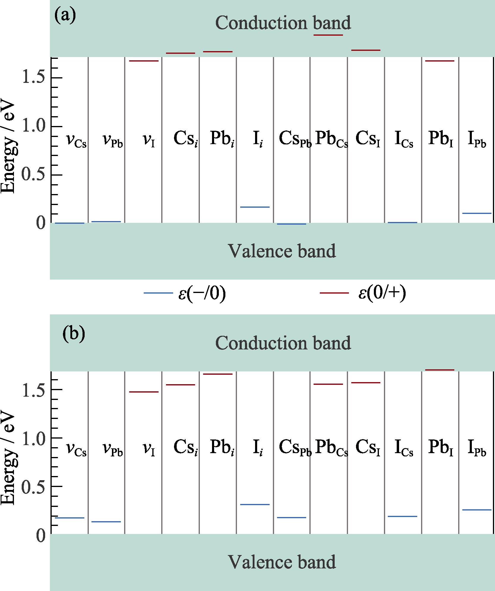
图 4.
Fig. 4. Defect transition levels in γ -CsPbI3 calculated by HSE-0.43 (a) and PBE0-0.2 (b)Blue lines: acceptor levels; Red lines: donor levels
To investigate the deep-level defects observed in the PBE0-0.2 calculation, Kohn-Sham levels of defect supercells obtained from two functionals were further compared. Six types of single acceptor and single donor defects with an unpaired electron (or hole) in their neutral state were selected, and the qualitative differences between the results of two functionals were clearly observed by examining the position of the unpaired electron (or hole) in Kohn-Sham energy levels. For the donor (or acceptor) defects, Fig. 5(a) shows the position of the unpaired electron (or hole) in the bandgap obtained from the HSE-0.43 calculation. For the typical shallow-level defects vCs, vI, Csi, and CsPb, the position of the unpaired electron (or hole) in the bandgap is very close to the band edge (i.e., VBM or CBM). However, for the PBE0-0.2 results in Fig. 5(b), the energy level positions of above four defects clearly enter the band gap, which is consistent with the appearance of deep DTL in Fig. 4(b).
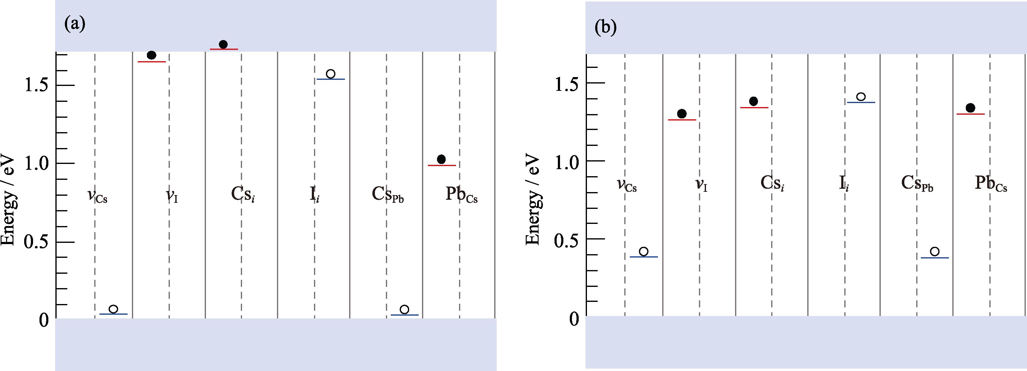
图 5.
Fig. 5. Kohn-Sham energy levels of v Cs, v I, Csi , Ii , CsPb and PbCs defects calculated by HSE-0.43 (a) and PBE0-0.2 (b)For acceptor defects, the left half is for −1 state, while the right half is for the neutral state. For donor defects, the left half is for neutral state, while the right half is for +1 state. Open and solid circles represent holes and electrons, respectively.
The cases of Ii and PbCs are more complicated. Previous studies have shown that Ii may have both acceptor and donor properties (i.e. amphoteric defect)[54]. The structural distortions of both defects are relatively large, which may lead to the appearance of deep-level defects. Both functionals in Fig. 4 give a deeper ε(−/0) level for Ii, and the result from PBE0-0.2 is slightly deeper. For the ε(0/+) level of PbCs, the result from HSE-0.43 is above CBM, indicating that the level is relatively shallow, while the result from PBE0-0.2 is deeper as shown in Fig. 4(b). Although the Kohn-Sham levels of PbCs in Fig. 5 are deep, its ε(0/+) level is not a deep-level defect, which is related to the detailed bonding situation of Pb at Cs site.
Comparing the results of two functionals, it is found that, relative to PBE0-0.2, although the proportion of Hartree-Fock exchange in HSE-0.43 is higher, it still gives correct results for typical shallow-level defects. The exchange interaction in Hartree-Fock calculations is a long-range interaction. In supercell calculations, the size of the supercell is usually not sufficient to avoid the interaction between the defect and its periodic images, which leads to a decrease in the energy level of the defect and its entry into the bandgap. This is the reason for the deep-level defects observed in PBE0-0.2[55]. In contrast, HSE-0.43 screens the long-range Hartree-Fock interaction and can avoid this problem even in a relatively small supercell of 160 atoms, as used in this study. In principle, PBE0-0.2 may also obtain shallower levels in larger supercells.
3 Conclusions
This study compared the performance of two main hybrid functional methods, HSE-0.43 and PBE0-0.2, in calculating the intrinsic defect properties of the orthorhombic phase CsPbI3. To accurately describe the band gap, all defect calculations considered the spin- orbit coupling effect, including structural relaxation. The properties of the bulk phase were firstly studied using two methods, and it was found that except for slight quantitative differences, their results were basically consistent. However, there were qualitative differences between the defect transition energy levels and Kohn- Sham energy levels obtained by two methods. The shallow energy levels obtained by HSE-0.43 were mostly converted to deep energy levels in PBE0-0.2 calculations. This result is attributed to the long-range interaction of the Hartree-Fock exchange potential, which cannot be avoided in PBE0-0.2 calculations using small-size supercells, while the HSE functional, which screens the long-range Hartree-Fock exchange potential, could obtain the converged defect properties using relatively small supercells. Therefore, the HSE functional is an efficient method for accurate prediction of the defect properties of halide perovskite materials, and eligible for the related design of photovoltaic, light-emitting and scintillation materials.
9 Supporting materials
Supporting materials related to this article can be found at
WU Xiaowei1, ZHANG Han1,2, ZENG Biao1,2, MING Chen1,2, SUN Yiyang1,2
(1. Shanghai Institute of Ceramics, Chinese Academy of Sciences, Shanghai 201899, China; 2. Center of Materials Science and Optoelectronics Engineering, University of Chinese Academy of Sciences, Beijing 100049, China)
Fig. S1 compares the density of states (DOS) obtained by the two methods. It can be seen that, except for the smaller valence band width obtained by PBE0-0.2, there are no other significant differences. Each peak on two total DOS curves can be corresponded to each other, but the peak positions are slightly shifted. From the decomposed DOS curves, it can be seen that the valence band is mainly contributed by the p orbitals of I, and the s orbitals of Pb also contribute near the valence band maximum (VBM). The conduction band minimum (CBM) is mainly contributed by the p orbitals of Pb.
Fig. S2 compares the effective masses of carriers obtained by two methods through parabolic fitting. CBM and VBM are taken as the energy reference points for the conduction and valence bands, respectively, for convenience of plotting. It can be seen that the energy bands near the Γ point can be well fitted by parabolas along three principal axes directions. The maximum difference in effective mass along three directions is about 0.1m0. The difference in effective masses of electrons and holes is also small, indicating a balanced electron-hole transport property of CsPbI3.
Fig. S3 shows the real and imaginary parts of the dielectric constant, respectively. Since the accurate calculation of dielectric constant requires a sufficient number of empty states and a sufficient high density of k-points, the PBE functional was first employed to test the convergence of the number of empty states and the density of k-points. The results showed that a 5×4×5 k-point grid and 544 empty states can converge the calculated dielectric constant to an accuracy of about 0.01. Figure S3 shows that there is a slight difference in the bulk dielectric constant calculated by the HSE-0.43 and PBE0-0.2 functionals. The difference is about 0.19 for ε1 at 0 eV and the slight lagging behind of ε2 calculated by HSE-0.43 is related to the slightly wider band gap obtained by this method.
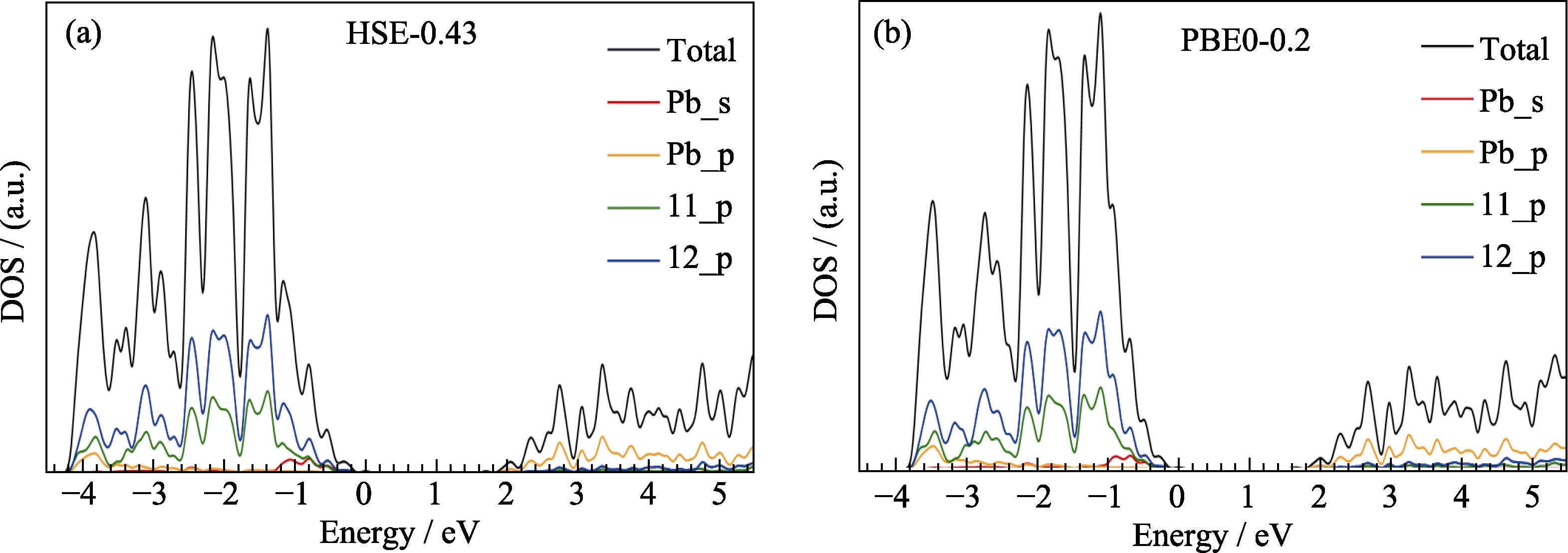
图 6.
Fig. 6. Total and projected density of states of γ-CsPbI3 calculated by two hybrid functionals HSE-0.43 (a) and PBE0- 0.2 (b) including the SOC effect
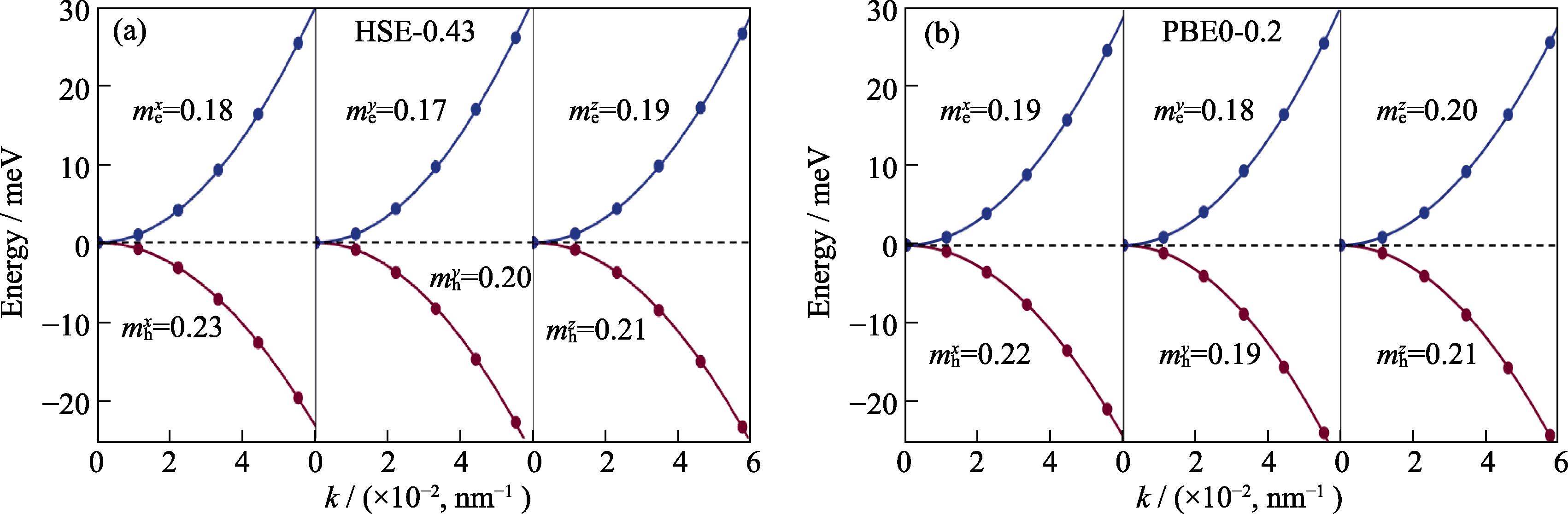
图 7.
Fig. 7. Parabolic fitting of the band near Γ point to obtained the effective masses of electrons and holes.For clarity, the electron and hole bands are referenced to the CBM and VBM, respectively; SOC effect is included here; (a) HSE-0.43; (b) PBE0-0.2
[5] SALIBA M, MATSUI T, DOMANSKI K, et al. Incorporation of rubidium cations into perovskite solar cells improves photovoltaic performance[J]. Science, 2016, 354: 206.
[9]
[10] BELIKOVICH B A, PASHCHUK I P, PIDZYRAILO N S. Luminescence of CsPbCl3 single-crystals[J]. Optikai I Spectroskopiya, 1977: 113.
[48] XIANG W, LIU S, TRESS W, et al. A review on the stability of inorganic metal halide perovskites: challenges and opportunities for stable solar cells[J]. Energy & Environmental Science, 2021, 14: 2090.
[51] BLÖCHL P. E.. Projector augmented-wave method[J]. Physical Review B, 1994, 50: 17953.
吴晓维, 张涵, 曾彪, 明辰, 孙宜阳. 杂化泛函HSE和PBE0计算CsPbI3缺陷性质的比较研究[J]. 无机材料学报, 2023, 38(9): 1110. Xiaowei WU, Han ZHANG, Biao ZENG, Chen MING, Yiyang SUN.


 PDF全文
PDF全文
