1 山东省科技服务发展推进中心,济南 250101
2 山东大学机械工程学院,济南 250061
作为典型的硬脆材料,氧化镓晶体(β-Ga2O3)加工时易裂解。金刚石线锯是生产β-Ga2O3晶片的主要方式,切片加工过程中会在晶片表面产生微裂纹损伤层,应力作用下微裂纹会发生扩展,导致材料破碎和断裂。本文建立了金刚石线锯多线切割β-Ga2O3(010)晶面的有限元模型,研究了锯切过程中机械应力、热应力和热力耦合应力的分布变化规律,分析了锯丝速度、进给速度和恒速比下不同参数组合对热力耦合应力的影响。结果表明,锯切过程中锯切热产生的热应力占据热力耦合应力的主导地位,锯切力引起的机械应力占比较小,但机械应力会影响热力耦合应力的分布情况,锯丝速度和进给速度的增加会引起热力耦合应力的增加。
金刚石线锯 有限元分析 热力耦合应力 机械应力 热应力 β-Ga2O3 β-Ga2O3 diamond wire saw finite element analysis thermal-mechanical coupling stress mechanical stress thermal stress
1 山东大学,新一代半导体材料研究院,晶体材料国家重点实验室,济南 250100
2 山东工业技术研究院,济南 250100
本文使用导模(EFG)法生长了Ni掺杂β-Ga2O3单晶,并通过粉末X射线衍射(PXRD)和劳厄衍射(Laue diffraction)分别验证了其晶体结构和晶体质量。进一步通过紫外-可见-近红外透过光谱及红外透过光谱研究了Ni2+掺杂对β-Ga2O3光学特性的影响,发现其(100)面的紫外截止边为252.9 nm,对应的光学带隙为4.74 eV。此外,阴极荧光(CL)光谱测试结果显示,Ni2+掺杂β-Ga2O3单晶在600~800 nm具有宽带近红外发光特性,有望拓宽β-Ga2O3单晶材料在宽带近红外方面的应用。
氧化镓 宽禁带半导体 光电性能 宽带近红外发光 导模法 Ni掺杂 Ga2O3 wide-bandgap semiconductor optical and electrical property broadband near-infrared luminescent EFG method Ni doping
Author Affiliations
Abstract
1 State Key Laboratory of Information Photonics and Optical Communications & School of Science, Beijing University of Posts and Telecommunications, Beijing 100876, China
2 Advanced Institute for Materials Research (WPI-AIMR), Tohoku University, Sendai 980-8577, Japan
3 Department of Engineering Science, Faculty of Innovation Engineering, Macau University of Science and Technology, Macau 999078, China
4 Institute of Modern Optics & Tianjin Key Laboratory of Micro-Scale Optical Information Science and Technology, Nankai University, Tianjin 300071, China
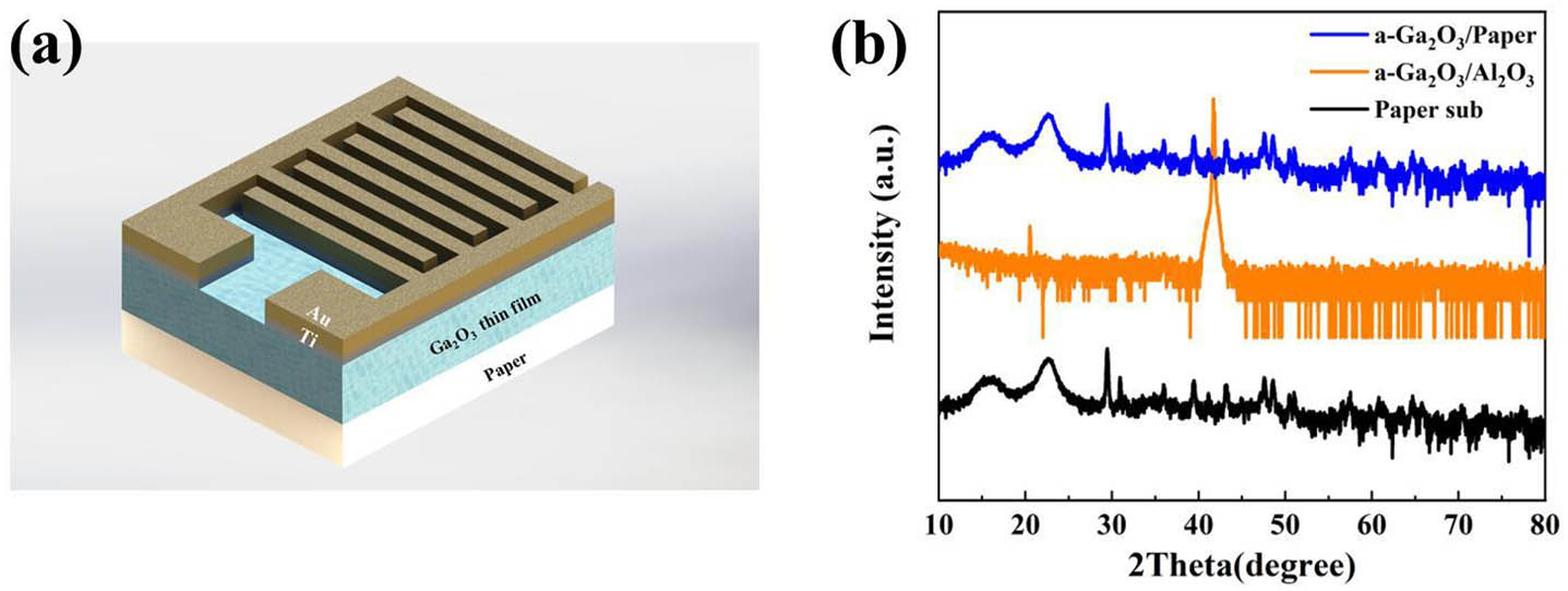
Flexible devices provide advantages such as conformability, portability, and low cost. Paper-based electronics offers a number of advantages for many applications. It is lightweight, inexpensive, and biodegradable, making it an ideal choice for disposable electronics. In this work, we propose a novel configuration of photodetectors using paper as flexible substrates and amorphous as the active materials, respectively. The photoresponse characteristics are investigated systematically. A decent responsivity yield and a specific detectivity of up to 66 mA/W and Jones were obtained at a low operating voltage of 10 V. The experiments also demonstrate that neither the twisting nor bending deformation can bring obvious performance degradation to the device. This work presents a candidate strategy for the application of conventional paper substrates to low-cost flexible solar-blind photodetectors, showing the potential of being integrated with other materials to create interactive flexible circuits.
amorphous Ga2O3 flexible photodetector solar-blindness paper Chinese Optics Letters
2023, 21(10): 101601
北京石油化工学院新材料与化工学院, 北京 102617
本文采用基于密度泛函理论的第一性原理计算了不同Al掺杂浓度β-Ga2O3(即(AlxGa1-x)2O3)的晶体结构、电荷密度分布、能带结构、态密度和光学性质, 并对本征β-Ga2O3和不同Al掺杂浓度的β-Ga2O3的计算结果进行了分析对比。结果表明, 随着Al掺杂浓度的增加, (AlxGa1-x)2O3的晶格常数和键长均单调减小, 而带隙逐渐增大。β-Ga2O3导带底上方存在主要由Ga 4s和Al 3p轨道组成的中间带, Al掺杂在此中间带引入杂质能级, 从而导致带隙增加。同时, Al的引入使态密度向高能侧偏移了近3 eV, 也导致了带隙的增加。根据光学性质的计算结果, 在掺杂Al后, 介电函数的虚部和吸收系数均观察到明显的蓝移现象。这是由价带顶中的O 2p态和导带底中的Ga 4s态之间的跃迁产生的。并且, 随着Al掺杂浓度的增加, 蓝移现象加剧。本文研究可为基于(AlxGa1-x)2O3光电器件的设计提供思路和理论指导。
第一性原理 掺杂 Al掺杂β-Ga2O3 能带结构 电子结构 光学性质 first-principle doping Al-doped β-Ga2O3 band structure electronic structure optical property
1 山东大学, 新一代半导体材料研究院, 晶体材料国家重点实验室, 济南 250100
2 山东工业技术研究院, 济南 250100
本文研究了斜切角的引入对β-Ga2O3(100)面衬底加工的影响, 分析了斜切角分别为0°、1°、6°时, (100)面衬底在加工过程中的形貌变化及不同抛光参数对衬底抛光的影响。实验结果表明, 随着斜切角的增大, (100)面衬底在加工过程中的解理损伤问题得以改善, 加工后表面粗糙度降低, 材料去除方式出现了脆性去除-脆塑性混合去除-塑性去除的转变。较小的抛光压力可以有效减少解理损伤, 改善表面质量。斜切角为6°时的(100)面衬底抛光效率高, 抛光后表面粗糙度可达到Ra≤0.2 nm。
解理 斜切角 抛光 表面粗糙度 β-Ga2O3 β-Ga2O3 cleavage miscut-angle polishing surface roughness
本文使用金属有机物化学气相沉积(MOCVD)法在不同切割角的c面蓝宝石衬底上外延氧化镓(β-Ga2O3)单晶薄膜, 揭示了衬底切割角对外延薄膜晶体质量的影响规律。研究表明, 当衬底切割角为6°时, β-Ga2O3外延膜具有较小的X射线摇摆曲线半峰全宽(1.10°)和最小的表面粗糙度(7.7 nm)。在此基础上, 采用光刻、显影、电子束蒸发及剥离工艺制备了金属-半导体-金属结构的日盲紫外光电探测器, 器件的光暗电流比为6.2×10⁶, 248 nm处的峰值响应度为87.12 A/W, 比探测率为3.5×10¹⁵ Jones, 带外抑制比为2.36×10⁴, 响应时间为226.2 μs。
超宽禁带半导体 氧化镓薄膜 金属有机物化学气相沉积 日盲紫外光电探测器 切割角 外延 ultra-wide bandgap semiconductor β-Ga2O3 film metal organic chemical vapor deposition solar-blind ultraviolet photodetector off-cut angle epitaxy

Author Affiliations
Abstract
Key Laboratory of Optical Field Manipulation of Zhejiang Province, Department of Physics, Zhejiang Sci-Tech University, Hangzhou 310018, China
Gallium oxide (Ga2O3) based flexible heterojunction type deep ultraviolet (UV) photodetectors show excellent solar-blind photoelectric performance, even when not powered, which makes them ideal for use in intelligent wearable devices. However, traditional flexible photodetectors are prone to damage during use due to poor toughness, which reduces the service life of these devices. Self-healing hydrogels have been demonstrated to have the ability to repair damage and their combination with Ga2O3 could potentially improve the lifetime of the flexible photodetectors while maintaining their performance. Herein, a novel self-healing and self-powered flexible photodetector has been constructed onto the hydrogel substrate, which exhibits an excellent responsivity of 0.24 mA/W under 254 nm UV light at zero bias due to the built-in electric field originating from the PEDOT: PSS/Ga2O3 heterojunction. The self-healing of the Ga2O3 based photodetector was enabled by the reversible property of the synthesis of agarose and polyvinyl alcohol double network, which allows the photodetector to recover its original configuration and function after damage. After self-healing, the photocurrent of the photodetector decreases from 1.23 to 1.21 μA, while the dark current rises from 0.95 to 0.97 μA, with a barely unchanged of photoresponse speed. Such a remarkable recovery capability and the photodetector’s superior photoelectric performance not only significantly enhance a device lifespan but also present new possibilities to develop wearable and intelligent electronics in the future.
Ga2O3 hydrogels self-powered self-healing UV photodetector Journal of Semiconductors
2023, 44(7): 072807
Author Affiliations
Abstract
School of Microelectronics, University of Science and Technology of China, Hefei 230026, China
We demonstrate superb large-area vertical β-Ga2O3 SBDs with a Schottky contact area of 1 × 1 mm2 and obtain a high-efficiency DC–DC converter based on the device. The β-Ga2O3 SBD can obtain a forward current of 8 A with a forward voltage of 5 V, and has a reverse breakdown voltage of 612 V. The forward turn-on voltage (VF) and the on-resistance (Ron) are 1.17 V and 0.46 Ω, respectively. The conversion efficiency of the β-Ga2O3 SBD-based DC–DC converter is 95.81%. This work indicates the great potential of Ga2O3 SBDs and relevant circuits in power electronic applications.
β-Ga2O3 SBD DC–DC converter Journal of Semiconductors
2023, 44(7): 072805


