为了进一步提升P-GaN 栅HEMT器件的阈值电压和击穿电压, 提出了一种具有P-GaN栅结合混合掺杂帽层结构的氮化镓高电子迁移率晶体管(HEMT)。新器件利用混合掺杂帽层结构, 调节整体极化效应, 可以进一步耗尽混合帽层下方沟道区域的二维电子气, 提升阈值电压。在反向阻断状态下, 混合帽层可以调节栅极右侧电场分布, 改善栅边电场集中现象, 提高器件的击穿电压。利用Sentaurus TCAD进行仿真, 对比普通P-GaN栅增强型器件, 结果显示, 新型结构器件击穿电压由593 V提升至733 V, 增幅达24%, 阈值电压由0509 V提升至1323 V。
氮化镓高电子迁移率晶体管 增强型 击穿电压 混合帽层 GaN HEMT enhancement-mode breakdown voltage hybrid cap layer

Author Affiliations
Abstract
1 Institute of Microelectronics, Chinese Academy of Sciences, Beijing 100029, China
2 University of Chinese Academy of Sciences, Beijing 100049, China
3 Suzhou Institute of Nano-Tech and Nano-Bionics, Chinese Academy of Sciences, Suzhou 215123, China
In this letter, an enhancement-mode (E-mode) GaN p-channel field-effect transistor (p-FET) with a high current density of ?4.9 mA/mm based on a O3-Al2O3/HfO2 (5/15 nm) stacked gate dielectric was demonstrated on a p++-GaN/p-GaN/AlN/AlGaN/AlN/GaN/Si heterostructure. Attributed to the p++-GaN capping layer, a good linear ohmic I?V characteristic featuring a low-contact resistivity (ρc) of 1.34 × 10?4 Ω·cm2 was obtained. High gate leakage associated with the HfO2 high-k gate dielectric was effectively blocked by the 5-nm O3-Al2O3 insertion layer grown by atomic layer deposition, contributing to a high ION/IOFF ratio of 6 × 10⁶ and a remarkably reduced subthreshold swing (SS) in the fabricated p-FETs. The proposed structure is compelling for energy-efficient GaN complementary logic (CL) circuits.
GaN p-FETs enhancement-mode HfO2 subthreshold swing Journal of Semiconductors
2023, 44(10): 102801
Author Affiliations
Abstract
1 State Key Laboratory of Electronic Thin Films and Integrated Devices, University of Electronic Science and Technology of China, Chengdu 610054, China
2 Key Laboratory of Nanodevices and Applications, Suzhou Institute of Nano-tech and Nano-bionics, CAS, Suzhou 215123, China
3 Institute of Electronic and Information Engineering, University of Electronic Science and Technology of China, Dongguan 523808, China
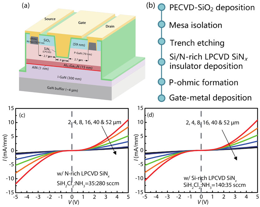
In this work, the GaN p-MISFET with LPCVD-SiNx is studied as a gate dielectric to improve device performance. By changing the Si/N stoichiometry of SiNx, it is found that the channel hole mobility can be effectively enhanced with Si-rich SiNx gate dielectric, which leads to a respectably improved drive current of GaN p-FET. The record high channel mobility of 19.4 cm2/(V?s) was achieved in the device featuring an Enhancement-mode channel. Benefiting from the significantly improved channel mobility, the fabricated E-mode GaN p-MISFET is capable of delivering a decent-high current of 1.6 mA/mm, while simultaneously featuring a negative threshold-voltage (VTH) of –2.3 V (defining at a stringent criteria of 10 μA/mm). The device also exhibits a well pinch-off at 0 V with low leakage current of 1 nA/mm. This suggests that a decent E-mode operation of the fabricated p-FET is obtained. In addition, the VTH shows excellent stability, while the threshold-voltage hysteresis ΔVTH is as small as 0.1 V for a gate voltage swing up to –10 V, which is among the best results reported in the literature. The results indicate that optimizing the Si/N stoichiometry of LPCVD-SiNx is a promising approach to improve the device performance of GaN p-MISFET.
p-channel GaN p-FET LPCVD channel mobility hole mobility enhancement-mode Journal of Semiconductors
2023, 44(8): 082801
Author Affiliations
Abstract
1 School of Nano Technology and Nano Bionics, University of Science and Technology of China, Hefei 230026, China
2 Nano Fabrication Facility, Suzhou Institute of Nano-Tech and Nano-Bionics, Chinese Academy of Sciences, Suzhou 215123, China
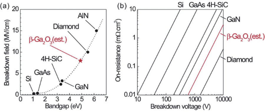
Power electronic devices are of great importance in modern society. After decades of development, Si power devices have approached their material limits with only incremental improvements and large conversion losses. As the demand for electronic components with high efficiency dramatically increasing, new materials are needed for power device fabrication. Beta-phase gallium oxide, an ultra-wide bandgap semiconductor, has been considered as a promising candidate, and various β-Ga2O3 power devices with high breakdown voltages have been demonstrated. However, the realization of enhancement-mode (E-mode) β-Ga2O3 field-effect transistors (FETs) is still challenging, which is a critical problem for a myriad of power electronic applications. Recently, researchers have made some progress on E-mode β-Ga2O3 FETs via various methods, and several novel structures have been fabricated. This article gives a review of the material growth, devices and properties of these E-mode β-Ga2O3 FETs. The key challenges and future directions in E-mode β-Ga2O3 FETs are also discussed.
enhancement mode FETs β-Ga2O3 Journal of Semiconductors
2023, 44(6): 061801
为获得更高的阈值电压, 提出了一种新型栅下双异质结增强型AlGaN/GaN高电子迁移率晶体管(HEMT)。使用双异质结电荷控制模型分析了基本机理, 推导了阈值电压表达式。仿真结果表明, 器件阈值电压与调制层Al组分呈线性关系。当调制层Al组分小于势垒层时, 阈值电压增大, 反之减小。调制层厚度可加大这种调制作用。当调制层Al组分为0%、厚度为112 nm时, 器件具有2.13 V的阈值电压和1.66 mΩ·cm2的比导通电阻。相对于常规凹槽栅结构, 新结构的阈值电压提高了173%。
增强型 高电子迁移率晶体管 阈值电压 双异质结 电荷控制模型 enhancement-mode HEMT threshold voltage double heterojunction charge control model
随着射频/微波器件的快速发展及其应用领域的日益扩大,基于半导体单片集成技术的多种器件集成工艺不断发展。研究了一种采用AlGaAs--InGaAs的砷化镓化合物衬底。琥珀酸湿法蚀刻工艺对器件电性能影响较小。将耗尽型和增强型赝配高电子迁移率晶体管(pseudomorphic High--Electron--Mobility Transistor, pHEMT)器件集成于同一芯片半导体工艺技术。结果表明,增强型晶体管Y型栅极的线宽为0.25 m,开启电压为0.3 V;耗尽型晶体管栅极的线宽为0.5 m,开启电压为-0.8 V,实现了在同一芯片上集成从负到正的栅极电压分布,为设计者提供了更为宽广的设计平台。这种集成技术可以应用于低噪声放大器、线性天线开关、滤波器以及功率控制装置等领域。
增强型 耗尽型 低噪声放大器 单片微波集成电路 二维电子气 enhancement-mode depletion-mode pHEMT pHEMT low noise amplifier monolithic microwave integrated circuit two-dimensional electron gas


