1 1.华东师范大学 物理与电子科学学院, 极化材料与器件教育部重点实验室, 上海 200241
2 2.中国科学院 上海硅酸盐研究所, 上海 200050
3 3. 山西大学 极端光学协同创新中心,太原 030006
宽禁带γ-CuI是一种具有优异光电和热电性能的p型透明半导体材料, 近年来受到广泛关注。但作为一种新兴材料, 其发光性能受材料缺陷影响的物理机理尚不清楚。本工作通过气相反应法制备了Cl掺杂的CuI薄膜, 采用电镜表征方法研究Cl掺杂对多晶CuI薄膜表面形貌和阴极荧光发光特性的影响, 并结合第一性原理计算探究了Cl在CuI薄膜中的主要存在形式, 以揭示Cl掺杂CuI薄膜结构与发光性能的联系。研究结果表明, 原本晶粒饱满但晶界显著的CuI薄膜掺杂Cl后呈现出致密平整的表面, 表明Cl掺杂剂改变了CuI的表面结构。相比未掺杂区域, Cl掺杂区410 nm处的荧光信号明显得到双倍增强, 而在720 nm附近的缺陷峰则略有降低, 说明Cl掺杂极大改善了CuI薄膜的发光性能。通过第一性原理计算对该现象进行理论分析, 发现引入Cl元素有效抑制了CuI中碘空位等深能级缺陷的产生, 降低了激子发生非辐射跃迁的概率, 从而改善CuI的发光性能, 这与阴极荧光的结果一致。本研究获得的掺杂CuI薄膜带边发光峰的半峰宽仅为7 nm, 表现出极高的发光单色性。这些发现有助于对卤素掺杂获得的高性能CuI基材料的理解。
CuI Cl掺杂 阴极荧光 第一性原理计算 CuI Cl-doping cathodoluminescence first principle calculation 
Author Affiliations
Abstract
1 School of Physics, Peking University, Beijing 100871, China
2 The State Key Laboratory for Artificial Microstructures and Mesoscopic Physics, School of Physics & Center for Quantitative Biology, Academy for Advanced Interdisciplinary Studies, Peking University, Beijing 100871, China
3 Academy for Advanced Interdisciplinary Studies, Peking University, Beijing 100871, China
4 Wenzhou Institute, University of Chinese Academy of Sciences, Wenzhou 325001, China
Chirality plays an important role in biological processes, and enantiomers often possess similar physical properties and different physiologic functions. In recent years, chiral detection of enantiomers become a popular topic. Plasmonic metasurfaces enhance weak inherent chiral effects of biomolecules, so they are used in chiral detection. Artificial intelligence algorithm makes a lot of contribution to many aspects of nanophotonics. Here, we propose a nanostructure design method based on reinforcement learning and devise chiral nanostructures to distinguish enantiomers. The algorithm finds out the metallic nanostructures with a sharp peak in circular dichroism spectra and emphasizes the frequency shifts caused by nearfield interaction of nanostructures and biomolecules. Our work inspires universal and efficient machine-learning methods for nanophotonic design.
chiral detection metasurface deep learning cathodoluminescence Opto-Electronic Science
2023, 2(1): 220019
Author Affiliations
Abstract
1 School of Physics, State Key Lab for Mesoscopic Physics, Academy for Advanced Interdisciplinary Studies, Collaborative Innovation Center of Quantum Matter, and Nano-optoelectronics Frontier Center of Ministry of Education, Peking University Yangtze Delta Institute of Optoelectronics, Peking University, Beijing 100871, China
2 National Laboratory of Solid State Microstructures, Department of Materials Science and Engineering, Nanjing University, Nanjing 210093, China
3 College of Chemistry and Molecular Engineering, Peking University, Beijing 100871, China
4 Department of Physics and HKU-UCAS Joint Institute for Theoretical and Computational Physics at Hong Kong, the University of Hong Kong, Pokfulam Road, Hong Kong, China
![]()
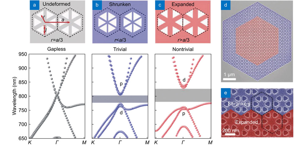
![]() Photonic topological insulators with robust boundary states can enable great applications for optical communication and quantum emission, such as unidirectional waveguide and single-mode laser. However, because of the diffraction limit of light, the physical insight of topological resonance remains unexplored in detail, like the dark line that exists with the crystalline symmetry-protected topological edge state. Here, we experimentally observe the dark line of the Z2 photonic topological insulator in the visible range by photoluminescence and specify its location by cathodoluminescence characterization, and elucidate its mechanism with the p-d orbital electromagnetic field distribution which calculated by numerical simulation. Our investigation provides a deeper understanding of Z2 topological edge states and may have great significance to the design of future on-chip topological devices.
Photonic topological insulators with robust boundary states can enable great applications for optical communication and quantum emission, such as unidirectional waveguide and single-mode laser. However, because of the diffraction limit of light, the physical insight of topological resonance remains unexplored in detail, like the dark line that exists with the crystalline symmetry-protected topological edge state. Here, we experimentally observe the dark line of the Z2 photonic topological insulator in the visible range by photoluminescence and specify its location by cathodoluminescence characterization, and elucidate its mechanism with the p-d orbital electromagnetic field distribution which calculated by numerical simulation. Our investigation provides a deeper understanding of Z2 topological edge states and may have great significance to the design of future on-chip topological devices.
photonic topological insulator edge state cathodoluminescence TMDC Opto-Electronic Advances
2022, 5(4): 210015
1 苏州科技大学 数理学院, 江苏省微纳热流技术与能源应用重点实验室, 江苏 苏州 215009
2 中国科学院苏州纳米技术与纳米仿生研究所, 江苏 苏州 215123
采用离子注入方法在氢化物气相外延法生长的AlN薄膜中注入了不同剂量的Dy3+和Eu3+,制备了Dy3+单掺、Dy3+和Eu3+共掺的AlN样品.对于Dy3+单掺杂AlN样品,X射线衍射和拉曼散射实验结果表明随着Dy注入剂量的增加,样品的压应力也增加,形成了比较明显的损伤层;但当注入剂量由5×10¹⁴ at/cm2增加至1×1015 at/cm2时,压应力增加不明显,接近于饱和.对于Dy3+和Eu3+共掺的AlN样品,阴极荧光实验表明,AlN中Eu3+和Dy3+之间可能存在能量传递,能量传递途径为在声子辅助下从Dy3+的4F9/2→6H15/2至Eu3+的7F0→5D2的共振能量传递.此外,计算发现改变Dy3+和Eu3+离子的注入剂量比能实现发光色度坐标和色温的有效调控.
光电子 氮化铝 应力 阴极荧光 能量传递 Optoe1ectronics Aluminum nitride Europium 铕 Dysprosium 镝 Strain Cathodoluminescence Energy transfer 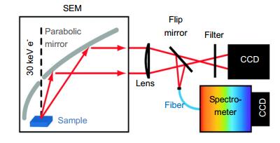
Author Affiliations
Abstract
School of Physics, State Key Lab for Mesoscopic Physics, Academy for Advanced Interdisciplinary Studies, Collaborative Innovation Center of Quantum Matter, Peking University, Beijing 100871, China
Cathodoluminescence (CL) as a radiative light produced by an electron beam exciting a luminescent material, has been widely used in imaging and spectroscopic detection of semiconductor, mineral and biological samples with an ultrahigh spatial resolution. Conventional CL spectroscopy shows an excellent performance in characterization of traditional material luminescence, such as spatial composition variations and fluorescent displays. With the development of nanotechnology, advances of modern microscopy enable CL technique to obtain deep valuable insight of the testing sample, and further extend its applications in the material science, especially for opto-electronic investigations at nanoscale. In this article, we review the study of CL microscopy applied in semiconductor nanostructures for the dislocation, carrier diffusion, band structure, doping level and exciton recombination. Then advantages of CL in revealing and manipulating surface plasmon resonances of metallic nanoantennas are discussed. Finally, the challenge of CL technology is summarized, and potential CL applications for the future opto-electronic study are proposed.
cathodoluminescence microscopy semiconductor metallic nanostructures surface plasmons Opto-Electronic Advances
2018, 1(4): 180007
1 江苏省微纳热流技术与能源应用重点实验室 苏州科技大学数理学院, 江苏 苏州 215009
2 中国科学院 苏州纳米技术与纳米仿生研究所, 江苏 苏州 215123
通过MOCVD方法在蓝宝石衬底上生长GaN薄膜, 利用离子注入方法将Eu3+离子注入到GaN基质中。X射线衍射结果表明: 经过退火处理后, 修复了部分离子注入所导致的晶格损伤。利用阴极荧光光谱可得到GaN∶Eu3+材料在623 nm处有很强的红光发射, 该发射峰来源于Eu3+离子的内部4f能级跃迁。另外, Eu3+离子注入会在样品中引入电荷转移态, 产生408 nm附近的发光。退火处理有助于获得更强的电荷转移态发光和Eu离子特征发光。GaN基质的黄光峰与Eu离子之间存在能量交换, 将能量传递给Eu离子, 促进Eu离子发光。
氮化镓 阴极荧光 铕 发光 能量传递 gallium nitride cathodoluminescence europium luminescence energy transfer
1 上海大学 材料科学与工程学院, 上海 200444
2 中国科学院苏州纳米技术与纳米仿生研究所, 江苏 苏州 215123
3 苏州科技大学 物理科学与技术系, 江苏 苏州 215009
采用离子注入法在GaN薄膜中实现了Er3+和Eu3+离子的共掺杂.以阴极荧光光谱仪为主要表征手段, 研究样品的光学特性和能量传递机理.在300 K温度下, Er3+和Eu3+共掺杂GaN薄膜能够实现绿光和红光的同时发射.随着Er3+离子掺杂剂量的增加, Eu3+离子相关发光峰的强度减弱, Er3+离子对应的两个相关发光峰强度比值减小, 表明Er3+和Eu3+离子之间发生了能量传递, 能量传递的方向为Eu3+→Er3+.变温阴极荧光光谱显示, Er3+离子的2H11/2和4S3/2两个能态相关的跃迁峰相对强度比值随着温度升高而降低, 主要是由两个能级之间的热耦合导致.改变Er3+离子的掺杂剂量, 能够调控GaN: Er3+/Eu3+样品的光学色度坐标和色温, 表明此材料可用于发光器件.
光电子学 阴极荧光 光学特性 能量传递 Optoelectronics GaN GaN Cathodoluminescence Optical properties Energy transfer
中国科学院上海技术物理研究所 红外成像材料与器件重点实验室, 上海 200083
利用Te熔剂方法,在天宫二号飞船上成功地生长了ZnTe:Cu晶体.微重力下生长的晶体质量优于地面生长的晶体,相同实验条件下,天宫二号上生长的晶体尺寸明显大于地面尺寸.通过阴极荧光光谱(CL)无损检测技术测试了5 kV、15 kV、25 kV高压下的ZnTe:Cu 晶体的阴极荧光图谱及光谱.
微重力 ZnTe:Cu晶体 阴极荧光光谱(CL) microgravity ZnTe:Cu crystal cathodoluminescence
1 苏州科技大学 数理学院 江苏省微纳热流技术与能源应用重点实验室,江苏 苏州 215009
2 中国科学院苏州纳米技术与纳米仿生研究所,江苏 苏州 215123
采用离子注入的方法在氮化铝(AlN)薄膜中实现Er3+和Pr3+的共掺杂,以阴极荧光光谱仪为主要表征手段,对其发光特性进行研究.对于Er3+单掺杂的AlN薄膜,在 410 nm和480 nm可以观察到Er3+较强的发光峰, 在 537 nm、560 nm、771 nm和819 nm可观察到Er3+的较弱的发光峰;对于Pr3+单掺杂的AlN薄膜,Pr3+的最强发光峰位于528nm, 在657 nm和675 nm可以观察到Pr3+的较弱的发光峰;而对于Er3+和Pr3+共掺杂的AlN薄膜,在494nm观察到与Pr3+相关的新跃迁峰.根据实验现象,对AlN薄膜中Er3+和Pr3+之间的能量传递机制进行了深入分析,结果表明Er3+的4F7/2→4I15/2能级跃迁与Pr3+的3P0→3H4能级跃迁之间发生了共振能量传递,从而使Pr3+产生了494nm新的发光峰.
光电子学 氮化铝 阴极荧光 饵 钋 发光 能量传递 Optoelectronics Aluminum nitride Cathodoluminescence Europium Polonium Luminescence Energy transfer


