光学学报, 2022, 42 (17): 1716001, 网络出版: 2022-09-16
宽禁带半导体光电材料及其应用研究  下载: 1515次特邀综述
Wide Band Gap Semiconductor Optoelectronic Materials and Their Applications
图 & 表
图 1. MOCVD法制备的p-ZnO薄膜和LED器件[4]。(a)ZnO发光二极管;(b)ZnO LED的I-V特性;(c)LED的室温电致发光光谱随注入电流的变化
Fig. 1. p-ZnO thin films and LED devices prepared by MOCVD method[4]. (a) Schematic sketch of ZnO LED; (b) I-V characteristics of ZnO LED; (c) electroluminescence spectra of LED as a function of injected current at room temperature
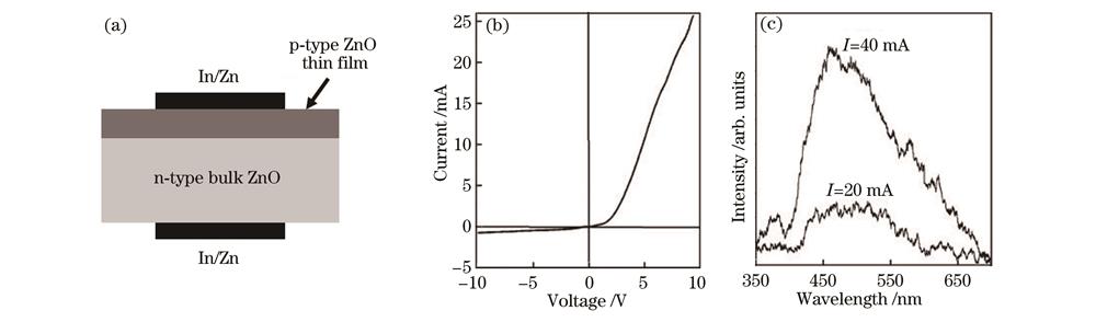
图 2. 能带结构示意图。(a)ZnMgO/ZnO[7];(b)ZnMgO/ZnMgBeO[11]
Fig. 2. Schematic diagrams of band structures. (a) ZnMgO/ZnO[7];(b)ZnMgO/ZnMgBeO[11]

图 3. 调控ZnO/ZnMgO多量子阱阱宽、垒高的PL强度。(a)温度为16 K时的PL强度;(b)室温下的PL强度;(c)归一化PL强度
Fig. 3. PL intensity obtained by adjusting well width and barrier height of ZnO/ZnMgO multi-quantum wells. (a) PL intensity at 16 K; (b) PL intensity at room temperature; (c) normalized PL intensity
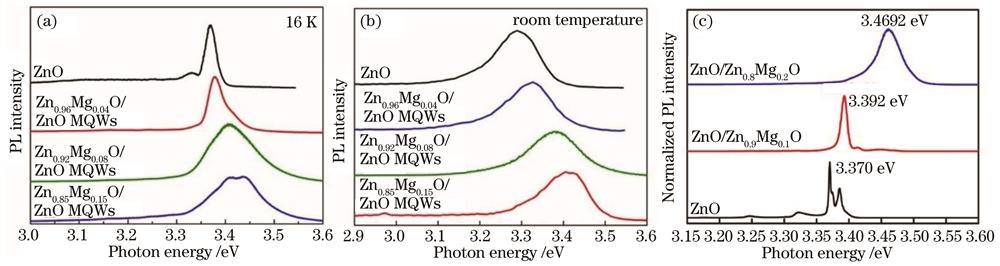
图 4. 高内量子效率ZnO/ZnMgO多量子阱的PL强度。(a)ZnO/Zn0.9Mg0.1O多量子阱生长在GaN/Al2O3衬底上80 K时的PL光谱(插图显示了多量子阱LE发射的综合PL强度作为温度的函数);(b)生长在蓝宝石衬底上的ZnO/Zn0.9Mg0.1O多量子阱在300 K和15 K下的PL光谱
Fig. 4. PL intensity of ZnO/ZnMgO multi-quantum wells with high internal quantum efficiency. (a) PL spectrum at 80 K of ZnO/Zn0.9Mg0.1O MQWs grown on GaN/Al2O3 substrate (inset shows integrated PL intensity of LE emission for MQWs as a function of temperature); (b) PL spectra at 300 K and 15 K of the ZnO/Zn0.9Mg0.1O MQWs grown on sapphire substrate
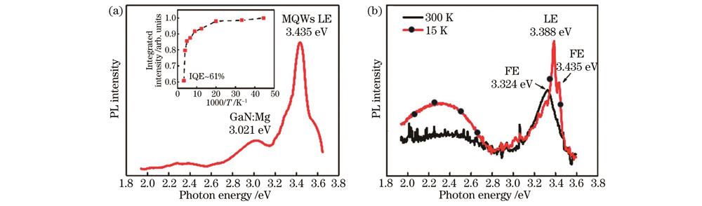
图 6. 钙钛矿发光研究结果。(a)(d)红光钙钛矿薄膜LED电致发光(EL)谱及最大EQE统计结果[117];(b)(e)绿光钙钛矿薄膜LED的EL谱及最大EQE统计结果[118];(c)(f)天蓝光钙钛矿薄膜LED的EL谱及最大EQE统计结果[107]
Fig. 6. Results of perovskite luminescence. (a)(d) Statistical results of electroluminescence (EL) spectrum and external quantum efficiency (EQE) of red perovskite film LED[117]; (b)(e) statistical results of EL spectrum and maximum EQE of green perovskite film LED[118]; (c)(f) statistical results of EL spectrum and maximum EQE of sky blue perovskite film LED[107]

图 7. 钙钛矿薄膜ASE结果。(a)(e)PMMA表层钝化绿光钙钛矿薄膜ASE结果[120];(b)(f)底层钝化和表层钝化绿光钙钛矿薄膜ASE结果[121];(c)结晶形貌优化后的绿光钙钛矿薄膜ASE结果[122];(d)蓝光钙钛矿薄膜ASE结果;(g)红绿光钙钛矿薄膜ASE激射;(h)蓝绿光钙钛矿薄膜ASE激射[123]
Fig. 7. ASE results of perovskite thin films. (a)(e) ASE results of green perovskite thin films with PMMA surface passivation[120]; (b)(f) ASE results of green perovskite thin films passivated in bottom and surface layers[121]; (c) ASE results of green light perovskite thin films after optimization of crystal morphology[122]; (d) ASE results of blue perovskite films; (g) ASE excitation results of red-green perovskite thin films; (h) ASE results of blue-green perovskite thin films[123]

图 8. 钙钛矿CsPbX3的能带结构、禁带宽度、光吸收谱和荧光光谱。(a)钙钛矿CsPbX3的能带结构示意图[124];(b)MAPbX3.的禁带宽度示意图[126];(c)CsPbX3纳米晶卤素组分依赖的光吸收谱和荧光光谱[129]
Fig. 8. Band structure, gap width, and absorption and fluorescence spectra of perovskite CsPbX3. (a) Schematic diagram of CsPbX3 band structure of perovskite[124]; (b) schematic diagram of gap width of MAPbX3[126]; (c) composition dependent light absorption and fluorescence spectra of CsPbX3 nanocrystalline halogen[129]

图 9. 纯溴基钙钛矿纳米粒子及其器件发光性能。(a)静电双壳层超小CsPbBr3蓝光量子点低倍TEM图和溶液示意图[133];(b)(c)刻蚀及配体交换处理后的超小CsPbBr3蓝光量子点TEM图和EL光谱图[134];(d)CsPbBr3纳米片TEM图[135];(e)(f)以CsPbBr3纳米片为发光层的LED器件性能图
Fig. 9. Luminescence properties of pure brominated perovskite nanoparticles and corresponding devices. (a) Low-power TEM and solution diagram of ultra-small CsPbBr3 blue quantum dots of electrostatic double shell [133]; (b)(c) TEM and EL spectra of ultra-small CsPbBr3 blue quantum dots after etching and ligand exchange treatment[134]; (d) TEM image of CsPbBr3 nanosheets[135]; (e)(f) performance diagram of LED device with CsPbBr3 nanosheet as luminescent layer

图 10. 纯溴基准二维钙钛矿及其器件发光性能。(a)准二维钙钛矿结构示意图和能量转移示意图[139];(b)准二维钙钛矿中不同间隔分子的排列方式示意图[140];(c)(d)两种间隔分子共存对准二维钙钛矿n值分布的影响及其器件EL光谱[141];(e)~(g)准二维钙钛矿钝化前后的光谱对比图和LED性能图[142]
Fig. 10. Luminescence properties of pure brominated quasi-two-dimensional perovskite nanoparticles and corresponding devices. (a) Schematic diagram of quasi-two-dimensional perovskite structure and energy transfer[139]; (b) schematic diagram of arrangement of different spacer molecules in quasi-two-dimensional perovskite[140]; (c)(d) effect of coexistence of two spacer molecules on n value distribution and EL spectra of quasi-two-dimensional perovskite[141]; (e)-(g) spectral contrast and LED performance before and after passivation of quasi-two-dimensional perovskite [142]
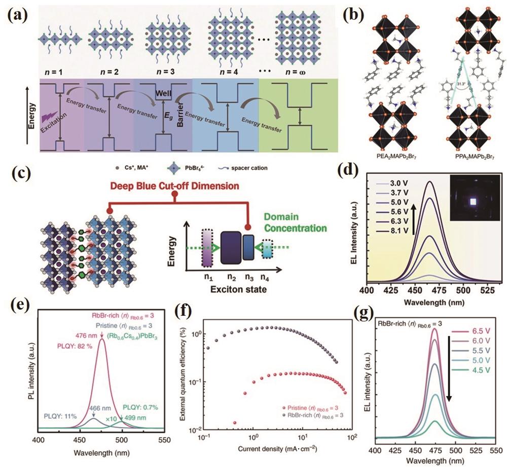
图 11. 混合卤素基钙钛矿纳米粒子及其器件发光性能。(a)配体钝化后的氯溴混合钙钛矿量子点溶液的荧光光谱图和紫外-可见光吸收光谱图[151];(b)氯溴混合钙钛矿量子点表面缺陷钝化示意图[152];(c)不同含量Ni+掺杂的氯溴混合钙钛矿量子点的发光示意图[153];(d)(e)Ni+掺杂前后氯溴混合钙钛矿量子点LED性能对比图[153]
Fig. 11. Luminescence properties of mixed halogen-based perovskite nanoparticles and corresponding devices. (a) Fluorescence and UV-visible absorption spectra of chlorobromine mixed perovskite quantum dot solution after ligand passivation[151]; (b) schematic diagram of surface defect passivation of chloro-bromine mixed perovskite quantum dots[152]; (c) luminescence diagram of different content Ni+ doped chloro-bromine mixed perovskite quantum dots[153]; (d)(e) comparison of LED performance of chloro-bromine mixed perovskite quantum dots before and after Ni+ doping[153]
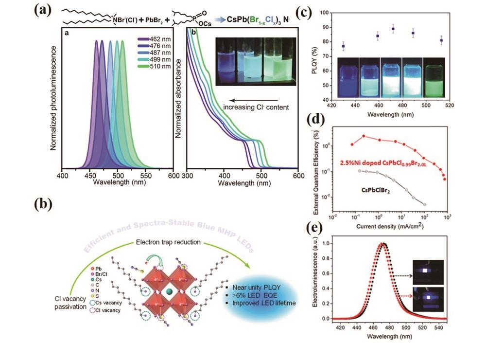
图 12. 混合卤素基准二维钙钛矿及其器件发光性能。(a)准二维钙钛矿配体钝化示意图[174];(b)不同间隔分子对准二维钙钛矿n值的影响[175];(c)不同间隔分子制备的准二维钙钛矿LED器件示意图[176];(d)不同氯溴比例的准二维钙钛矿禁带宽度示意图[180]
Fig. 12. Luminescence properties of mixed halogen-based perovskite and corresponding devices. (a) Schematic diagram of passivation of quasi-two-dimensional perovskite ligand[174]; (b) effect of different spacer molecules on n value of two-dimensional perovskite[175]; (c) schematic diagram of quasi-two-dimensional perovskite LED devices prepared by different spacer molecules[176]; (d) schematic diagram of quasi-two-dimensional perovskite bandgap width with different chloro-bromine ratios[180]

叶志镇, 王凤志, 陈芳, 陆杨丹. 宽禁带半导体光电材料及其应用研究[J]. 光学学报, 2022, 42(17): 1716001. Zhizhen Ye, Fengzhi Wang, Fang Chen, Yangdan Lu. Wide Band Gap Semiconductor Optoelectronic Materials and Their Applications[J]. Acta Optica Sinica, 2022, 42(17): 1716001.


 PDF全文
PDF全文

