中国激光, 2021, 48 (4): 0401007, 网络出版: 2021-02-08
高能激光单晶硅反射镜纳米精度控形控性制造技术  下载: 1372次特邀综述
Nanoprecision Control of Shape and Performance Manufacturing Technology for High-Energy Laser Silicon Components
图 & 表
图 1. 单晶硅超精密磨削后的缺陷深度。(a)初始表面,深度为0;(b)深度为1.5 μm;(c)深度为2.5 μm;(d)深度为3 μm
Fig. 1. Defect depth distribution after ultra-precision grinding of single crystal silicon. (a) Original surface, depth is 0; (b) depth is 1.5 μm; (c) depth is 2.5 μm; (c) depth is 3 μm
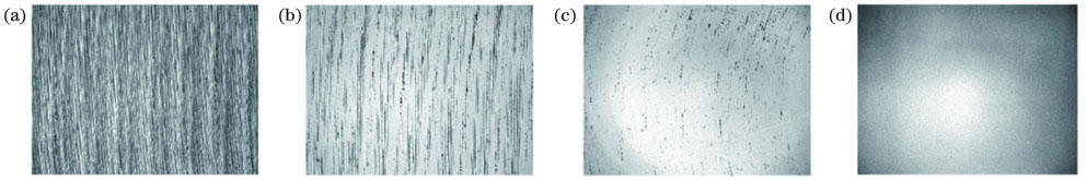
图 2. 单晶硅磁流变抛光。(a)加工中;(b)加工后
Fig. 2. Single crystal silicon magnetorheological polishing. (a) Polishing process; (b) after polishing
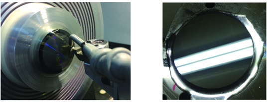
图 3. 柱面光顺工艺[17]。(a)柱面光顺实物图;(b)半刚性柱面光顺盘;(c)光顺前的局部中频误差;(d)光顺后的局部中频误差
Fig. 3. Cylindrical smoothing process[17]. (a) Practical equipment for cylindrical smoothing process; (b) semi-rigid cylindrical smoothing plate; (c) mid spatial frequency error before smoothing; (d) mid spatial frequency error after smoothing

图 4. 传统抛光与浸没式抛光。(a)传统抛光装置;(b)浸没式抛光装置
Fig. 4. Traditional polishing and immersion polishing equipment. (a) Traditional polishing equipment; (b) immersion polishing equipment
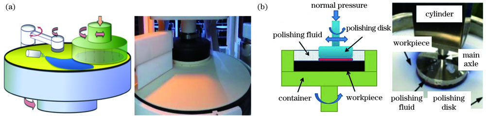
图 5. 通过大颗粒隔离实现的表面缺陷抑制。(a)空气中抛光,表面划痕;(b)空气中抛光,表面凸线;(c)浸没式抛光,表面无缺陷
Fig. 5. Surface defect suppression realized by isolating large particles. (a) Scratches on polished surfaces in air; (b) convex line on polished surfaces in air;(c) immersive polishing, without surface defects
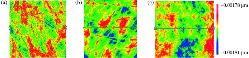
图 6. 离子束加工设备与物理溅射过程示意图[22]。(a)离子束加工设备;(b)物理溅射过程示意图
Fig. 6. Ion beam processing equipment and physical sputtering process. (a) Ion beam processing equipment; (b) physical sputtering process

图 7. 离子束倾斜入射实验[23]。 (a)实验照片;(b)工件面形误差分布
Fig. 7. Tilted incident experiments of ion beam[23]. (a) Experimental photo; (b) surface error map

图 8. 组合工艺路线。(a)浸没式抛光;(b)离子束修形;(c)面形精度测量
Fig. 8. Combined process route. (a) Immersion polishing; (b) ion beam figuring; (c) profile accuracy measurement
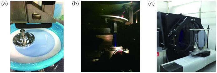
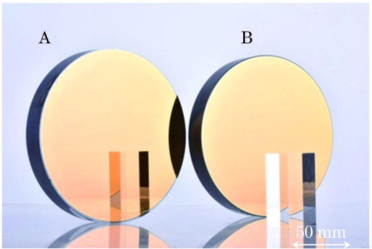
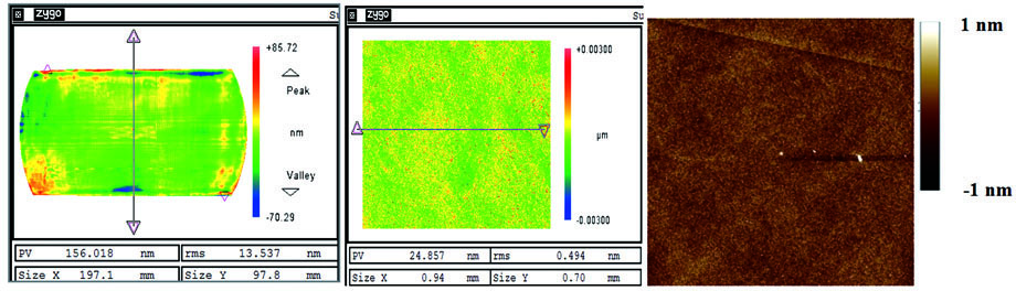
图 11. 凸柱面镜的加工结果。(a)低频面形误差RMS为13.537 nm;(b)中频面形误差RMS为0.494 nm;(c)高频面形误差RMS为0.261 nm
Fig. 11. Processing results of convex cylindrical mirror. (a) RMS of low spatial frequency surface shape error is 13.537 nm; (b) RMS of middle spatial frequency surface shape error is 0.494 nm; (c) RMS of high spatial frequency surface shape error is 0.261 nm
石峰, 田野, 乔硕, 周光奇, 宋辞, 薛帅, 铁贵鹏, 周林, 舒勇, 周港. 高能激光单晶硅反射镜纳米精度控形控性制造技术[J]. 中国激光, 2021, 48(4): 0401007. Feng Shi, Ye Tian, Shuo Qiao, Guangqi Zhou, Ci Song, Shuai Xue, Guipeng Tie, Lin Zhou, Yong Shu, Gang Zhou. Nanoprecision Control of Shape and Performance Manufacturing Technology for High-Energy Laser Silicon Components[J]. Chinese Journal of Lasers, 2021, 48(4): 0401007.


 PDF全文
PDF全文

