
Author Affiliations
Abstract
1 State Key Laboratory of Functional Materials for Informatics, Shanghai Institute of Microsystem and Information Technology, Chinese Academy of Sciences, Shanghai 200050, China
2 University of Chinese Academy of Sciences, Beijing 100049, China
3 School of Future Technology, University of Chinese Academy of Sciences, Beijing 100049, China
Here, we designed a broadband, low loss, compact, and fabrication-tolerant silicon-based four-mode edge coupler, composed of a adiabatic mode-evolution counter-taper splitter and a triple-tip inverse taper. Based on mode conversion and power splitting, the proposed structure can simultaneously realize efficient mode coupling from , , , and modes of multimode silicon waveguides to linearly polarized (LP), , , , and , modes in the few-mode fiber. To the best of our knowledge, we proposed the first scheme of four LP modes coupling, which is fully compatible with standard fabrication process. The 3D finite-difference time-domain simulation results show that the on-chip conversion losses of the four modes remain lower than 0.62 dB over the 200 nm wavelength range, and total coupling losses are 4.1 dB, 5.1 dB, 2.1 dB, and 2.9 dB for , , , and , respectively. Good fabrication tolerance and relaxed critical dimensions make the four-mode edge coupler compatible with standard fabrication process of commercial silicon photonic foundries.
multimode coupling CMOS compatibility silicon waveguide few-mode fiber Chinese Optics Letters
2022, 20(1): 011302
1 中国科学院上海微系统与信息技术研究所, 上海 200050
2 中国科学院大学, 北京 100049
上海市青年科技启明星计划(No.19QA1410600),上海市优秀学术带头人计划(No. 19XD1404600),中科院计划(No.Y82BRA1001)
量子存储 自组装量子点 单光子源 量子调控 应力调节 Quantum memory Self-assembled quantum dots Single-photon sources Quantum manipulation Strain tuning
1 中国科学院 上海微系统与信息技术研究所 信息功能材料国家重点实验室, 上海 200050
2 中国科学院大学, 北京100049
刻蚀衍射光栅(EDG)作为实现波分复用功能的关键器件, 对于片上光互连的实现至关重要。为了实现1310nm波段通道间隔为20nm的硅基EDG, 采用了基尔霍夫标量衍射理论仿真方法进行理论设计和仿真验证, 通过在闪耀光栅反射面引入布喇格反射光栅来提高反射效率、降低器件插入损耗, 并在入射波导处引入多模干涉耦合器以实现通道频谱平坦化设计。结果表明, 闪耀光栅反射面的反射效率由35%提高到了85%, 1dB带宽达到12nm。这对于提高系统稳定性、增大传输距离和容量、降低系统成本具有显著作用, 能够满足光互连系统的实际应用需求。
集成光学 刻蚀衍射光栅 硅基光互连 波分复用技术 integrated optics etching diffraction grating silicon-based optical interconnection wavelength division multiplex
Author Affiliations
Abstract
1 State Key Laboratory of Functional Materials for Informatics, Shanghai Institute of Microsystem and Information Technology, Shanghai 200050, China
2 Nantong Opto-Electronics Engineering Center Chinese Academy of Science, Nantong 226000, China
3 University of Chinese Academy of Science, Beijing 100049, China
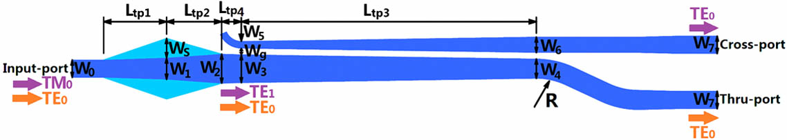
An ultra-broadband and fabrication-tolerant silicon polarization rotator splitter is proposed in this Letter. Benefitting from the broadband and low-loss characteristics of the bi-level taper and counter-tapered coupler, the designed device has a simulated insertion loss and crosstalk of less than 0.2 and 15 dB in the waveband from 1290 to 1610 nm. These characteristics make it valuable in applications with large bandwidth requirements, such as full-grid Coarse wavelength division multiplexer (CWDM) and diplexer/triplexer fiber-to-the-home systems. The fabrication tolerance of the design is also analyzed, showing that the device performance is quite stable with normal manufacturing errors in silicon photonics foundries.
130.3120 Integrated optics devices 130.5440 Polarization-selective devices Chinese Optics Letters
2016, 14(8): 081301


