1 河南仕佳光子科技股份有限公司, 河南 鹤壁 458030
2 中国科学院半导体研究所 半导体材料科学重点实验室, 北京 100083
为了应对共封装光学(CPO)系统对硅光外置光源提出的高功率、低噪声、低功耗等要求, 设计了一种波长在1310nm附近的AlGaInAs多量子阱(MQW)高功率连续波(CW)分布反馈(DFB)激光器芯片。通过在有源层MQW的下方插入一层InGaAsP远场减小层, 实现光模场向n型包层下移, 减小远场发散角的同时降低了量子阱区的光限制因子和整体的光吸收损耗, 制作的激光器可以实现高斜率效率、非致冷高温高功率工作。测试结果显示, 该激光器在25℃下, 阈值电流为20mA, 斜率效率为0.46W/A, 输出功率为173mW@400mA; 当注入电流为300mA时, 激光器的水平和竖直发散角分别是15.2°和19.1°, 边模抑制比大于55dB, 洛伦兹线宽小于600kHz, 相对强度噪声(RIN)小于-155dB/Hz; 在85℃高温下, 激光器阈值电流为32mA, 输出功率达到112mW@400mA。
共封装光学 连续波 多量子阱 分布反馈激光器 co-packaged optics (CPO) continuous wave (CW) multiple quantum well (MQW) AlGaInAs AlGaInAs distributed feedback (DFB) laser
1 商洛学院 化学工程与现代材料学院, 陕西 商洛 726000
2 南昌大学 材料科学与工程学院, 江西 南昌 330031
3 南昌大学 国家硅基LED工程技术研究中心, 江西 南昌 330047
4 安徽工业大学 数理科学与工程学院, 安徽 马鞍山 243032
利用MOCVD在Al2O3(0001)衬底上制备InGaN/GaN MQW结构蓝光LED外延片。以400 mW中心波长405 nm半导体激光器作为激发光源, 采用自主搭建的100~330 K低温PL谱测量装置, 以及350~610 K高温PL测量装置, 测量不同温度下PL谱。通过Gaussian分峰拟合研究了InGaN/GaN MQW主发光峰、声子伴线峰、n-GaN黄带峰峰值能量、相对强度、FWHM在100~610 K范围的温度依赖性。研究结果表明:在100~330 K温度范围内, 外延片主发光峰及其声子伴线峰值能量与FWHM温度依赖性, 分别呈现S与W形变化; 载流子的完全热化分布温度约为150 K, 局域载流子从非热化到热化分布的转变温度为170~190 K; 350~610 K高温范围内, InGaN/GaN MQW主发光峰峰值能量随温度变化满足Varshni经验公式, 可在MOCVD外延生长掺In过程中, 通过特意降温在线测PL谱, 实时推算掺In量, 在线监测外延片生长。以上结果可为外延片的PL发光机理研究、高温在线PL谱测量设备开发、掺In量的实时监测等提供参考。
多量子阱 发光二极管 外延 光致发光 GaN GaN MQW LED epitaxial photoluminesecence
Author Affiliations
Abstract
1 Laboratory of Micro-Nano Photonic and Optoelectronic Materials and Devices, Key Laboratory of Materials for High-Power Laser, Shanghai Institute of Optics and Fine Mechanics, Chinese Academy of Sciences, Shanghai 201800, China
2 Center of Materials Science and Optoelectronics Engineering, University of Chinese Academy of Sciences, Beijing 100049, China
3 State Key Laboratory of Surface Physics, Key Laboratory of Micro and Nano Photonic Structures of Ministry of Education, Department of Physics, Collaborative Innovation Center of Advanced Microstructures, Fudan University, Shanghai 200433, China
4 Department of Physics, Engineering Physics & Astronomy and Department of Chemistry, Queen’s University, Kingston K7L-3N6, Ontario, Canada
5 State Key Laboratory of High Field Laser Physics, Shanghai Institute of Optics and Fine Mechanics, Chinese Academy of Sciences, Shanghai 201800, China
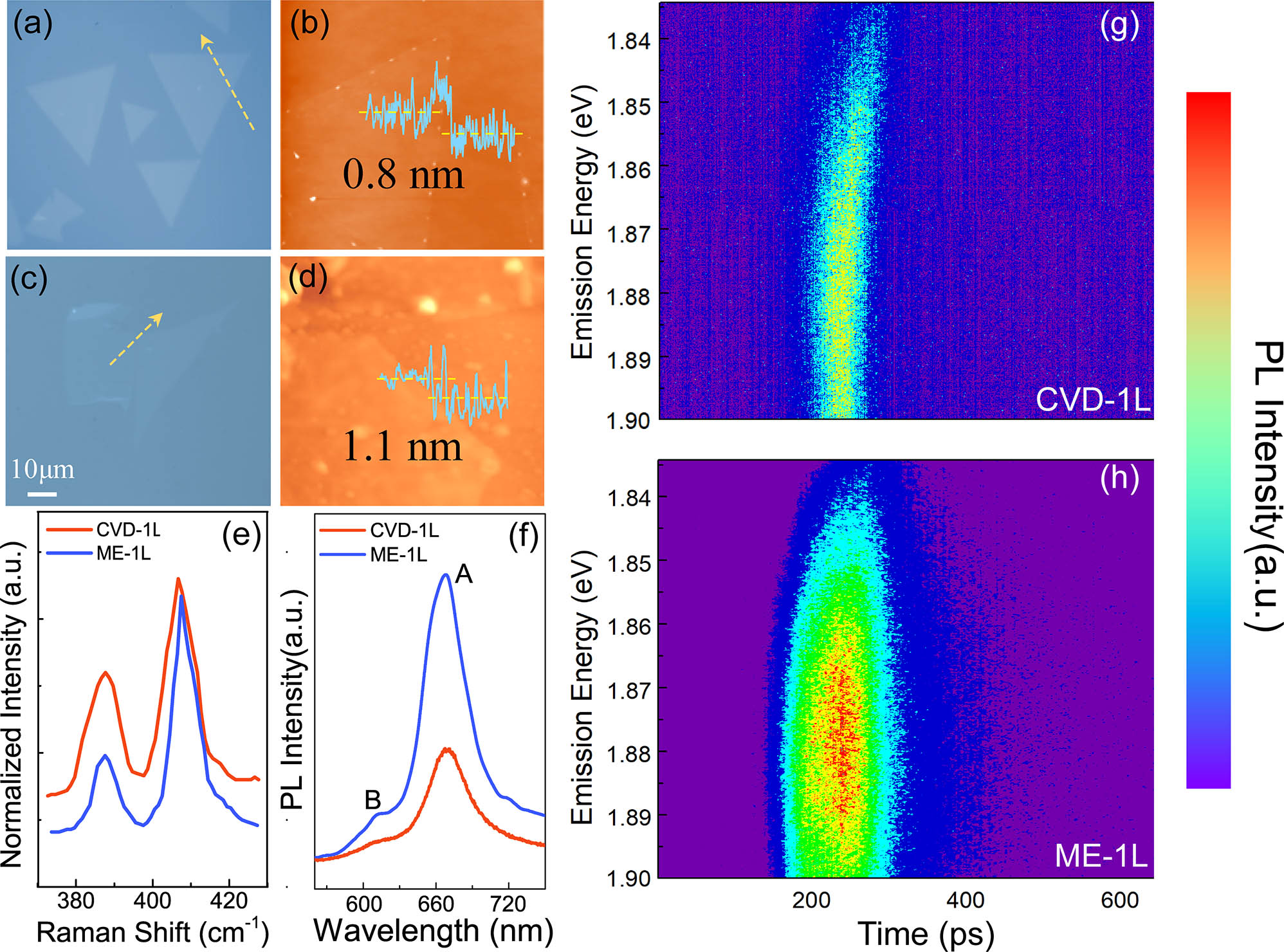
Mechanical exfoliation (ME) and chemical vapor deposition (CVD) MoS2 monolayers have been extensively studied, but the large differences of nonlinear optical performance between them have never been clarified. Here, we prepared MoS2 monolayers using ME and CVD methods and investigated the two-photon absorption (TPA) response and its saturation. We found that the TPA coefficient of the ME monolayer was about (1.88 ± 0.21) × 103 cm/GW, nearly two times that of the CVD one at (1.04 ± 0.15) × 103 cm/GW. Furthermore, we simulated and compared the TPA-induced optical pulse modulation in multilayer cascaded structures, which is instructive and meaningful for the design of optical devices such as a beam shaper and optical limiter.
190.4400 Nonlinear optics, materials 160.4236 Nanomaterials 190.5970 Semiconductor nonlinear optics including MQW 020.4180 Multiphoton processes Chinese Optics Letters
2019, 17(8): 081901

Author Affiliations
Abstract
1 Science and Technology on Monolithic Integrated Circuits and Modules Laboratory, Nanjing Electronic Devices Institute, Nanjing 210016, China
2 Key Laboratory of Semiconductor Materials Science, Institute of Semiconductors, Chinese Academy of Sciences, Beijing 100083, China
In this Letter, we reported the preliminary results of an integrating periodically capacitive-loaded traveling wave electrode (CL-TWE) Mach–Zehnder modulator (MZM) based on InP-based multiple quantum well (MQW) optical waveguides. The device configuration mainly includes an optical Mach–Zehnder interferometer, a direct current electrode, two phase electrodes, and a CL-TWE consisting of a U electrode and an I electrode. The modulator was fabricated on a 3 in. InP epitaxial wafer by standard photolithography, inductively coupled plasma dry etching, wet etching, electroplating, etc. Measurement results show that the MZM exhibits a 3 dB electro-optic bandwidth of about 31 GHz, a Vπ of 3 V, and an extinction ratio of about 20 dB.
130.3120 Integrated optics devices 250.4110 Modulators 230.4205 Multiple quantum well (MQW) modulators Chinese Optics Letters
2019, 17(6): 061301
1 厦门大学 物理系, 福建省半导体材料及应用重点实验室, 半导体光电材料及其高效转换器件协同创新中心, 福建 厦门 361005
2 中国科学院半导体研究所 半导体材料科学重点实验室, 北京 100083
紫外LED的发光功率和效率还远不能令人们满意,波长短于300 nm的深紫外LED的发光效率普遍较低。厘清高Al组分AlGaN多量子阱结构的发光机制将有利于探索改善深紫外LED的发光效率的新途径、新方法。为此,本文通过金属有机气相外延技术外延生长了表面平整、界面清晰可辨且陡峭的高Al组分AlGaN多量子阱结构材料,并对其进行变温光致发光谱测试,结合数值计算,深入探讨了AlGaN量子阱的发光机制。研究表明,量子阱中具有很强的局域化效应,其发光和局域激子的跳跃息息相关,而发光的猝灭则与局域激子的解局域以及位错引起的非辐射复合有关。
多量子阱结构 深紫外LED 发光机制 AlGaN AlGaN MQW deep UV-LED emission mechanism
Author Affiliations
Abstract
1 Department of Green Energy and Semiconductor Engineering, Hoseo University, Asan 330-713, South Korea
2 Department of Engineering Physics, McMaster University, Hamilton, Ontario L8S4L8, Canada
In this Letter, blue phosphorescence organic light-emitting diodes (PHOLEDs) employ structures for electron and/or hole confinement; 1,3,5-tris(N-phenylbenzimiazole-2-yl)benzene is used as a hole confinement layer and tris-(phenylpyrazole)iridium [Ir(ppz)3] is utilized for an electron confinement layer (ECL). The electrical and optical properties of the fabricated blue PHOLEDs with various carrier-confinement structures are analyzed. Structures with a large energy offset between the carrier confinement and emitting layers enhance the charge-carrier balance in the emitting region, resulting from the effective carrier confinement. The maximum external quantum efficiency of the blue PHOLEDs with the double-ECLs is 24.02% at 1500 cd/m2 and its luminous efficiency is 43.76 cd/A, which is 70.47% improved compared to the device without a carrier-confinement layer.
230.3670 Light-emitting diodes 230.0230 Optical devices 230.4170 Multilayers 230.4205 Multiple quantum well (MQW) modulators 230.5590 Quantum-well, -wire and -dot devices Chinese Optics Letters
2015, 13(3): 032301
长春理工大学 高功率半导体激光国家重点实验室,吉林 长春 130022
利用LASTIP软件理论分析了有源区量子阱数目对不同组分的InGaAsSb/AlGaAsSb 2 μm半导体激光器能带、电子与空穴浓度分布以及辐射复合率等性能参数的影响。研究表明:量子阱的个数是影响激光器件性能的关键参数,需要综合分析和优化。量子阱数太少时,量子阱对电子束缚能力弱,电子在p层中泄漏明显,辐射复合率低。量子阱数过多时,载流子在阱内分配不均匀,p型层中电子浓度升高,器件内损耗加大,辐射复合率下降。结合对外延材料质量的分析,InGaAsSb/AlGaAsSb 半导体激光器有源区最优量子阱数目为2~3。该研究结果可合理地解释已有实验报道,并为2 μm半导体激光器结构设计提供理论依据。
多量子阱激光器 有源区量子阱数目 数值模拟 MQW laser quantum well number in the active region numerical simulation
Author Affiliations
Abstract
1 Shanghai Institute of Optics and Fine Mechanics, Chinese Academy of Sciences, Shanghai 201800, China
2 University of Chinese Academy of Sciences, Beijing 100049, China
With the development of semiconductor technology, semiconductor laser devices and semiconductor laser pump solid-state laser devices have been widely applied in z-scan experiments. However, the feedback light-induced output instability of semiconductor laser devices can negatively affect the accurate testing of the nonlinear index. In this work, the influence of feedback light on z-scan measurement is analyzed. Then the calculated formula of feedback light-induced false nonlinear z-scan curves is theoretically derived and experimentally verified. Two methods are proposed to reduce or eliminate the feedback light-induced false nonlinear effect. One is the addition of an attenuator to the z-scan optical path, and the other is the addition of an opto-isolator unit to the z-scan setup. The experimental and theoretical results indicate that the feedback light-induced false nonlinear effect is markedly reduced and can even be ignored if appropriate parameters are chosen. Thus, theoretical and experimental methods of eliminating the negative effect of feedback light on z-scan measurement are useful for accurately obtaining the nonlinear index of a sample.
Nonlinear optics Semiconductor nonlinear optics including MQW Photonics Research
2014, 2(2): 02000051
1 大连理工大学 物理与光电工程学院, 辽宁 大连 116024
2 吉林大学电子科学与工程学院 集成光电子学国家重点实验室, 吉林 长春 130012
在Aixtron 3×2近耦合喷淋式金属有机化学气相沉积反应室中, 调节喷淋头与基座之间的距离, 制备了7, 13, 18, 25 mm间距的4个InGaN/GaN量子阱样品。利用原子力显微镜(AFM)、X射线衍射(XRD)对样品表面形貌及界面质量进行了表征。研究表明: 随着高度的增加, 量子阱的表面粗糙度减少, 垒/阱界面陡峭度逐步变差, 垒层和阱层厚度及阱层In组分含量减少; 增加高度至一定值后, 量子阱厚度及In组分趋于稳定。此外, 对比垒层和阱层的厚度变化, 垒层厚度的变化幅度较阱层更为明显。
高度调节 InGaN/GaN量子阱 MOCVD MOCVD showerhead gap position InGaN/GaN MQW
Author Affiliations
Abstract
1 College of Materials Science and Engineering, Taiyuan University of Technology, Taiyuan 030024, China
2 Key Laboratory of Interface Science and Engineering in Advanced Materials, Taiyuan University of Technology, Ministry of Education, Taiyuan 030024, China
The omni-directional reflection characteristics of one-dimensional photonic crystals composed of Ta2O5/MgF2 multi-quantum well (MQW) are studied using the transfer matrix method. An omni-directional reflector consisting of three and four Ta2O5/MgF2 MQWs is investigated. Results show that the photonic band gap of the photonic crystal composed of three and four Ta2O5/MgF2 MQWs, which are within the wavelength ranges of 402–712 and 412–1,023 nm, respectively, could cover the entire visible region. The relationship among the width of the band gap, its location, reflectivity rate, and incident angle of the incident light is analyzed. The optimal structural parameters of the MQW of the omni-directional reflector in the visible region are also calculated. The calculations provide a guide for the design of omni-directional reflection devices in the visible region.
光子晶体 传输矩阵方法 量子阱 全方位反射 可见光波段 160.5298 Photonic crystals 230.4205 Multiple quantum well (MQW) modulators 310.4165 Multilayer design 230.4040 Mirrors Chinese Optics Letters
2011, 9(7): 071603


