光电工程, 2023, 50 (3): 220048, 网络出版: 2023-05-04
飞秒激光双光子聚合三维微纳结构加工技术  下载: 683次
Femtosecond laser two-photon polymerization three-dimensional micro-nanofabrication technology
图 & 表
图 1. 单光子吸收、双(多)光子吸收、多光子电离及引发光聚合过程示意图[45-47]
Fig. 1. Schematic diagram of one-photon absorption, two (multi-) photon absorption, multi-photon ionization, and photopolymerization process[45-47]
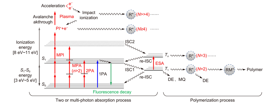
图 2. 光聚合交联过程及单体转化度。(a) 光刻胶中单体分子聚合和交联过程示意图[64]; (b) 在商业(丙烯酸酯基)光刻胶 IP-L 780 中不同扫描速度下拉曼光谱计算的单体转化度[67]
Fig. 2. Cross-linking process and degree of conversion. (a) Schematic diagram of the polymerization and cross-linking process of monomer molecules[64]; (b) Degree of conversion calculated from the Raman spectra for TPP with different scanning velocities in the commercial (acrylate-based) photoresist IP-L 780[67]
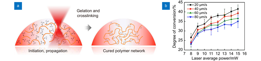
图 3. 光聚合阈值和破坏阈值分布图。(a) 激光曝光阈值强度随着曝光时间变化关系[71];(b) 暗场显微镜测量的不同扫描速度下聚合阈值和破坏阈值激光强度[47];(c) 暗场和原位显微镜测量单次和多次曝光下阈值激光强度[47]
Fig. 3. Distribution of the photopolymerization threshold and the damage threshold. (a) Laser exposure threshold intensity as a function of exposure time[71]; (b) Laser power threshold at different scan speeds measured by darkfield microscopy[47]; (c) Threshold laser intensities at single and multiple exposures measured by darkfield and in situ microscopy[47]
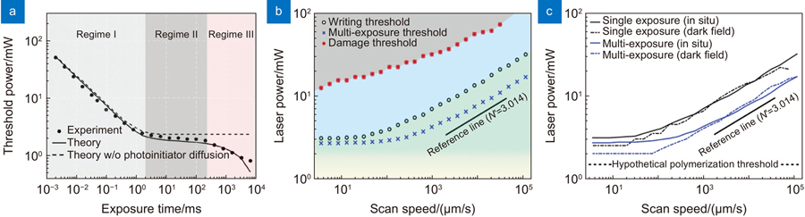
图 4. 双光子聚合加工超衍射特征尺寸结构,以及加工聚合体元(Voxel)形貌模型。(a) 双光子聚合加工示意图[15];(b) 制备的“纳米牛”[19];(c) 线宽与曝光时间的非线性关系[19];(d) 双光子聚合加工焦点处光强度分布,其中虚线为光强度的平方[47];(e) 体元长度与曝光功率关系[78];(f) 体元线宽与曝光功率关系[78]
Fig. 4. Sub-diffractive feature-scale structures by TPP and topography models of Voxel. (a) Schematic diagram of the TPP[15]; (b) The prepared "nano bull"[19]; (c) The nonlinear relationship between line width and exposure time[19]; (d) Light intensity distribution of the focus, where the dotted line is the square of light intensity[47]; (e) The relationship between voxel length and exposure power[78]; (f) The relationship between voxel linewidth and exposure power[78]
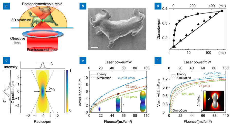
图 5. 双光子聚合加工系统示意图。(a) 典型的基于压电位移台扫描的双光子加工系统光路图[49];(b) 不同加工衬底对应不同的扫描策略示意图[17];(c) 振镜扫描、(d) 浸入式扫描、(e) 基于STED技术和 (f) 基于SLM的双光子加工系统示意图[17]
Fig. 5. Schematic diagram of the TPP system. (a) Optical path diagram of a typical TPP based on the piezoelectric stage scanning[49]; (b) Schematic diagram of different scanning strategies on different substrates[17]; (c) Galvanometer scanning, (d) immersion scanning, (e) STED assised and (f) SLM based TPP system[17]

图 6. 双光子聚合加工极限尺度纳米点、线结构。(a) 120 nm[19]、(b) 100 nm[98]、(c) 80 nm[100]、(d) 90 nm[101]、(e) 50 nm[103]、(f) 35 nm[74]、(g) 30 nm[104]、(h) 23 nm[105]、(i) 7 nm、8 nm和9 nm[106]特征尺度纳米点、线结构
Fig. 6. The nanodots/wires structures fabricated by TPP.(a) 120 nm[19], (b) 100 nm[98], (c) 80 nm[100], (d) 90 nm[101], (e) 50 nm[103], (f) 35 nm[74], (g) 30 nm[104], (h) 23 nm[105], (i) 7 nm, 8 nm and 9 nm[106] feature size in the nanodots/wires structures
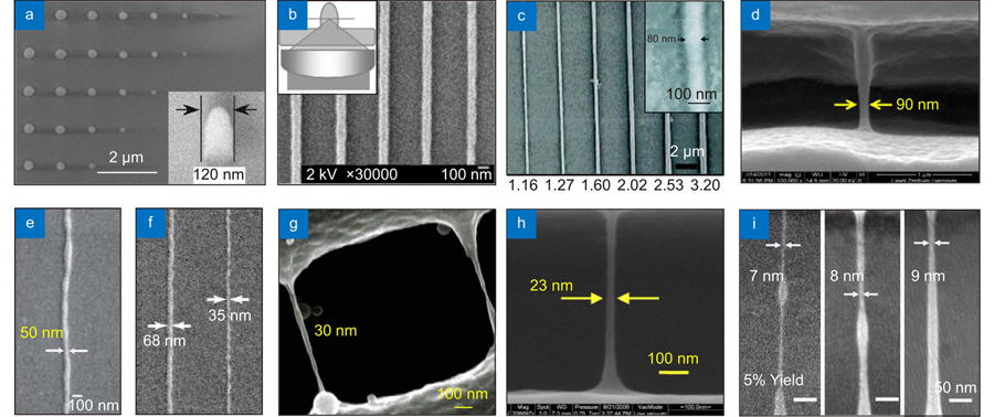
图 7. 基于STED双光子聚合加工极限尺度纳米线结构。(a) 基于STED双光子加工示意图及制备的结构最小纵向尺寸40 nm[110];(b) 纳米线线宽与532 nm 连续激光抑制光束功率的关系图及制备的95 nm、65 nm、90 nm和145 nm宽度的纳米线[111];(c) 聚合光束和抑制光束截面强度分布图,及制备的54 nm宽度纳米线[112];(d) 通过增加抑制光强提高分辨力的原理图及加工的9 nm特征尺度纳米线结构[113]
Fig. 7. The nanowires structures fabricated by STED-TPP. (a) Schematic diagram of the STED-TPP and the minimum longitudinal size of 40 nm[110]; (b) The relationship between the line width and the 532 nm CW laser and the fabricated nanowires with widths of 95 nm, 65 nm, 90 nm, and 145 nm[111]; (c) Cross-sectional intensity distributions of the initiation and inhibition laser beam, and the fabricated nanowires with width of 54 nm[112]; (d) Schematic diagram of improving resolution by increasing inhibition intensity and the fabricated nanowires with the minimum size of 9 nm[113]
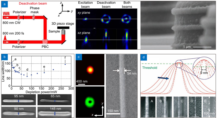
图 8. 基于多光束并行加工制备的周期性三维结构。(a,b) 基于衍射元件直写加工的微齿轮和微米牛组合结构[120];(c) 基于DMD投影拼接的二维阵列结构[121];(d) 基于SLM直写加工的抛物面镜结构[122];(e-g) 基于衍射元件直写加工三维力学超材料[123]
Fig. 8. Periodic 3D structures fabricated based on multi-beam parallel fabrication technology.(a,b) Micro-gear and micro-bull combined structures fabricated by TPP with diffractive elements[120]; (c) 2D array structure fabricated by TPP with DMD projection[121]; (d) Parabolic mirror structure based on SLM-TPP[122]; (e-g) 3D mechanical metamaterials fabricated by TPP with diffractive elements[123]
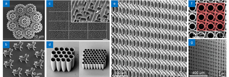
图 9. 基于DMD双光子加工制备的高精度、大尺寸结构。(a) DMD全息多焦点3D双光子打印方法,及打印的高分辨“桥”结构,二元全息产生单焦点、双焦点、三焦点制备的木堆结构[125];(b) 基于DMD飞秒投影双光子光刻技术及制备的具有亚微米特征尺度的厘米级三维结构,微纳悬臂结构[126];(c) 基于时空聚焦DMD投影双光子光刻技术及制备的微纳悬线结构,宏观超材料结构[127];(d) 基于DMD飞秒面投影纳米光刻技术及制备的纳米线、点结构,跨尺度微纳结构[128]
Fig. 9. High-precision, large-scale structures fabricated by DMD TPP technology.(a) DMD holographic multi-focus 3D TPP method and the fabricated high-resolution "bridge" structure, and woodpile structures[125]; (b) The prepared Millimeter-scale structure with sub-micrometer features, micro-nano bridge structures by FP-TPL technology[126]; (c) The prepared micro-nano suspended lines and micro-metamaterial structures by projection TPP with the spatiotemporal focusing technology[127]; (d) The prepared nanowires and nanodots structures, cross-scale structures by femtosecond projection nanolithography technology[128]
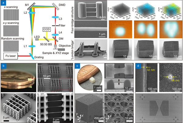
图 10. 光子晶体、超材料与器件。(a) 木堆结构光子晶体[131];(b) 金刚石结构光子晶体[133];(c) 热收缩的木堆光子晶体[134];(d) 手性螺旋超材料[135];(e) 光波段的三维隐身衣结构[136];(f) 光束偏转器[137];(g) 复合手性光子晶体材料[138];(h) 圆偏振光分光器[139]
Fig. 10. Photonic crystals, metamaterials, and devices. (a) Woodpile photonic crystal[131]; (b) Diamond photonic crystal[133]; (c) Heat shrinkable woodpile photonic crystal[134]; (d) Chiral helical metamaterial[135]; (e) 3D invisibility cloak structure in optical band[136]; (f) Beam deflector[137]; (g) Composite chiral photonic crystal material[138]; (h) Circularly polarized beam splitter[139]
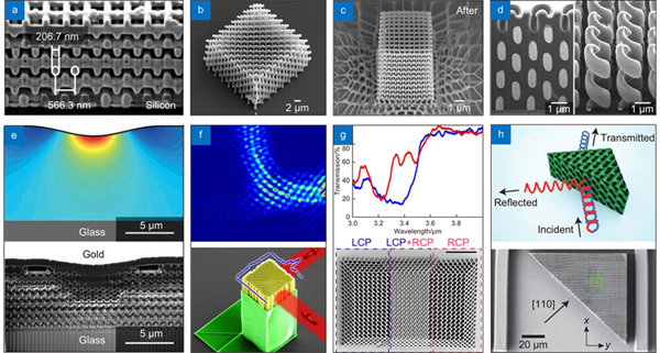
图 11. 超表面透镜器件。(a) 混合消色差超透镜宽带聚焦示意图[141];(b) 混合消色差超透镜的结构图[141];(c) 局部放大图[141];(d) 宽带近红外光成像效果[141];(e) 基于纳米孔相位板的宽带超透镜[142];(f) 测量的宽带聚焦光斑[142];(g) 可调焦距的 3D 双级联超透镜[146];(h) 测量的变焦距聚焦光斑[146]
Fig. 11. Metalens device. (a) Schematic diagram of the broadband focusing of the hybrid achromatic metalens[141]; (b) The structure of the hybrid achromatic metalens[141]; (c) The partial enlarged view[141]; (d) The imaging of the broadband near-infrared light[141]; (e) The broadband metalens, which combines nanoholes with a phase plate[142]; (f) Measured broadband focusing spot[142]; (g) The tunable multifocal 3D metalens[146]; (h) Measured zoom focusing spot[146]
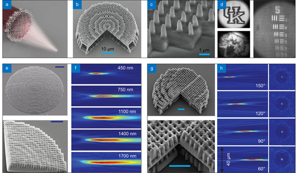
图 12. 集成光子学器件。(a) 微型棱镜耦合器[148];(b) 低损耗光纤-片上耦合器[149];(c) 偏振旋转的聚合物矩形波导[150];(d) 光纤-片上连接器[153];(e) 芯片-芯片光连接器[153];(f) 片上器件-器件光连接器[153];(g) 微盘腔结构和光互联波导结构[154];(h) 三维弯曲表面光子微腔结构[155]
Fig. 12. Integrated photonics device. (a) Miniature prism coupler[148]; (b) Low-loss fiber-on-chip coupler[149]; (c) Polarization-rotated polymer rectangular waveguide[150]; (d) Fiber-on-chip connector[153]; (e) Chip-on-chip optical connector[153]; (f) On-chip device-device optical connector[153]; (g) Microdisk cavity structure and optical interconnect waveguide structure[154]; (h) 3D curved surface photonic microcavity structure[155]
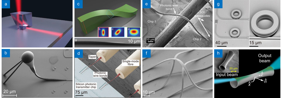
图 13. 微纳光学透镜。(a) 非球面固体浸没微透镜[158];(b) 超紧凑型多镜头物镜[159];(c) 堆叠衍射微透镜[160];(d) 渐变折射率龙伯透镜[161]
Fig. 13. Micro-nano optical lens. (a) Aspherical solid immersion microlenses[158]; (b) Ultracompact multi-lens objectives[159]; (c) Stacked diffractive microlenses[160]; (d) Graded index Lumberg lenses[161]
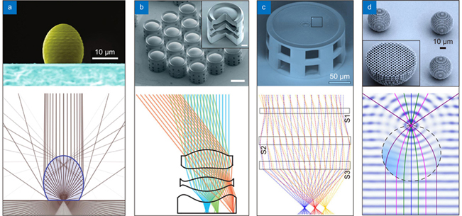
图 14. 逆向设计微纳光学器件。(a) 自由形式近红外偏振分束器[163];(b) 光谱分离超表面透镜[164];(c) 3D圆对称超透镜[165];(d) 多层超透镜[166]
Fig. 14. Inverse-designed micro-nano optics devices. (a) Free-form NIR polarizing beamsplitter[163]; (b) Spectral splitting metalens[164]; (c) 3D circularly symmetric metalens[165]; (d) Multilayer metalens[166]
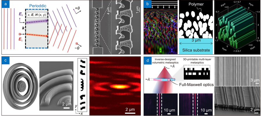
图 15. 力学超材料结构与器件。(a) 剪切模量消隐的五模式反膨胀力学超材料及上下两个直径不同相连接的双圆锥结构单元[168];(b) 无触感的弹性机械波斗篷[170];(c) 扭转机械超材料[171]
Fig. 15. Mechanical metamaterial structures and devices.(a) Pentamode metamterials and structural unit of two connected truncated cones[168]; (b) An elasto-mechanical unfeelability cloak made of metamaterials[170]; (c) A twist mechanical metamaterials[171]
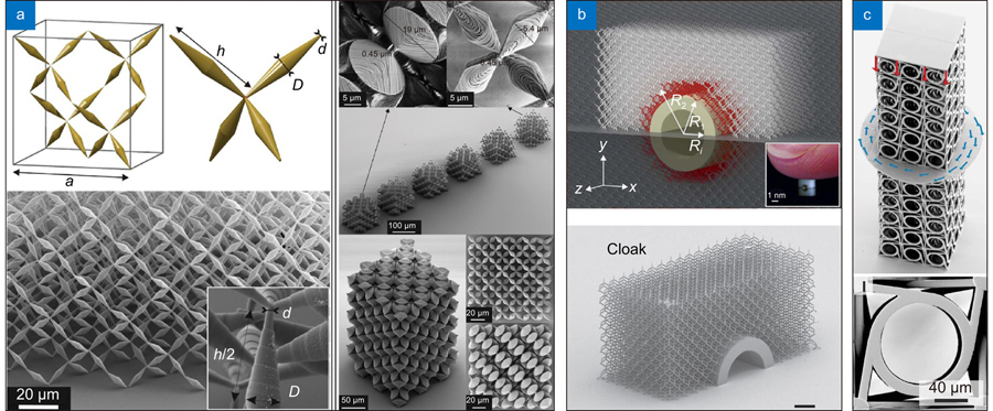
图 16. 可驱动的微机械器件。(a) 可远程磁驱动的微型转子、微型盾构机和三维螺旋推进器[176];(b) pH响应蜘蛛微型机器人和智能微型抓手[179];(c) 基于液晶弹性体的微型步行者[180];(d) 基于光镊驱动的微机械转子[181-182]
Fig. 16. Drivable micromechanical devices. (a) Remote magnetically actuated micro-rotor, micro-shield machine and 3D helical thruster[176]; (b) The pH-responsive spider micro-robot and smart micro-gripper[179]; (c) The liquid crystal elastomer-based micro-walker[180]; (d) Optical tweezers-driven micromechanical rotor[181-182]

图 17. 微流道器件。(a) 微泵[185];(b) 微涡轮[186];(c) 微筛[188];(d) 微过滤器[189];(e) 微阀门[190];(f) 微混合器[191];(g) 微混合器和过滤器[191];(d) 微立交桥器件[192]
Fig. 17. Microfluidic device. (a) Micropump[185]; (b) Microturbines[186]; (c) Microsieves[188]; (d) Microfilters[189]; (e) Microvalve[190]; (f) Micromixer[191]; (g) Micromixer and filters[191]; (d) Micro-overpass devices[192]
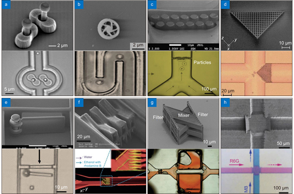
表 1两种不同聚合机理对比表[11, 46, 54]
Table1. Comparison of two different polymerization mechanisms [11, 46, 54]
|
赵圆圆, 金峰, 董贤子, 郑美玲, 段宣明. 飞秒激光双光子聚合三维微纳结构加工技术[J]. 光电工程, 2023, 50(3): 220048. Yuanyuan Zhao, Feng Jin, Xianzi Dong, Meiling Zheng, Xuanming Duan. Femtosecond laser two-photon polymerization three-dimensional micro-nanofabrication technology[J]. Opto-Electronic Engineering, 2023, 50(3): 220048.


 PDF全文
PDF全文
